- 您现在的位置:买卖IC网 > PDF目录45328 > MK1418S 24.576 MHz, OTHER CLOCK GENERATOR, PDSO8 PDF资料下载
参数资料
| 型号: | MK1418S |
| 元件分类: | 时钟产生/分配 |
| 英文描述: | 24.576 MHz, OTHER CLOCK GENERATOR, PDSO8 |
| 封装: | SOIC-8 |
| 文件页数: | 3/4页 |
| 文件大小: | 29K |
| 代理商: | MK1418S |
MK1418/MK1420
OPL3, OPL4 + Codec Clock Source
MDS 1418/20 A
3
Revision 013098
Printed 11/15/00
MicroClock Division of ICS1271 Parkmoor Ave.San JoseCA95126(408)295-9800tel(408)295-9818fax
Notes:
1. Stresses beyond those listed under Absolute Maximum Ratings could cause permanent damage to the device. Prolonged exposure
to levels above the operating limits but below the Absolute Maximums may affect device reliability.
2. Typical values are at 25°C.
3. If crystal is used as input with CL = 16pf. If a clock is used as input, the duty cycle of the 14.318MHz output will be the same as the
input clock.
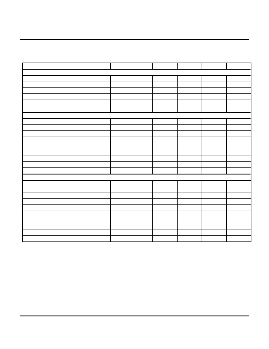
Electrical Specifications
Parameter
Conditions
Minimum
Typical
Maximum
Units
ABSOLUTE MAXIMUM RATINGS (note 1)
Supply Voltage, VDD
Referenced to GND
7
V
Inputs
Referenced to GND
-0.5
VDD+.5V
V
Clock Outputs
Referenced to GND
-0.5
VDD+.5V
V
Ambient Operating Temperature
0
70
°C
Soldering Temperature
Max of 20 seconds
260
°C
Storage temperature
-65
150
°C
DC CHARACTERISTICS (at 5.0V unless otherwise noted)
Operating Voltage, VDD
4.5
5.5
V
Input High Voltage, VIH
3.5
2.5
V
Input Low Voltage, VIL
2.5
1.5
V
Output High Voltage, VOH
IOH=-4mA
VDD-0.4
V
Output High Voltage, VOH
IOH=-25mA
2.4
V
Output Low Voltage, VOL
IOL=25mA
0.4
V
Operating Supply Current, IDD
No Load
18
mA
Input Capacitance
7
pF
Actual Mean Frequency versus Target
Outputs
±0.2
%
AC CHARACTERISTICS
Input Clock or Crystal Frequency
14.31818
MHz
Input Clock Duty Cycle, 14.318MHz
Time above 2.5V
20
80
%
Output Clock Rise Time
0.8 to 2.0V
1.5
ns
Output Clock Fall Time
2.0 to 0.8V
1.5
ns
Output Clock Duty Cycle, 24.576MHz
Time above 1.5V
40
45
60
%
Output Clock Duty Cycle, 16.9344 MHz
Time above 1.5V
45
50
55
%
Output Clock Duty Cycle, 33.868MHz
Time above 1.5V
45
50
55
%
Output Clock Duty Cycle, 14.318 MHz, Note 3
Time above 1.5V
45
50
55
%
Absolute Clock Period Jitter, except 14.3
Pins 4, 5, 6 only
-400
200
400
ps
One Sigma Clock Period Jitter, except 14.3
Pins 4, 5, 6 only
60
ps
相关PDF资料 |
PDF描述 |
|---|---|
| MK1491-06SLF | 49.152 MHz, PROC SPECIFIC CLOCK GENERATOR, PDSO28 |
| MK1491-06RLFTR | 49.152 MHz, PROC SPECIFIC CLOCK GENERATOR, PDSO28 |
| MK1491-06SLFTR | 49.152 MHz, PROC SPECIFIC CLOCK GENERATOR, PDSO28 |
| MK1492-02RLF | 75 MHz, PROC SPECIFIC CLOCK GENERATOR, PDSO28 |
| MK1492-02R | 75 MHz, PROC SPECIFIC CLOCK GENERATOR, PDSO28 |
相关代理商/技术参数 |
参数描述 |
|---|---|
| MK1418STR | 制造商:ICS 制造商全称:ICS 功能描述:OPL3, OPL4 + Codec Clock Source |
| MK14-1A66B-100W | 制造商:MEDER 制造商全称:Meder Electronic 功能描述:MK Reed Sensors |
| MK14-1A66B-100W_DE | 制造商:MEDER 制造商全称:Meder Electronic 功能描述:(deutsch) MK Reed Sensor |
| MK14-1A66B-1200W | 制造商:MEDER 制造商全称:Meder Electronic 功能描述:MK Reed Sensors |
| MK14-1A66B-1200W_09 | 制造商:MEDER 制造商全称:Meder Electronic 功能描述:MK Reed Sensor |
发布紧急采购,3分钟左右您将得到回复。