- 您现在的位置:买卖IC网 > PDF目录80577 > MK1434S 100 MHz, PROC SPECIFIC CLOCK GENERATOR, PDSO16 PDF资料下载
参数资料
| 型号: | MK1434S |
| 元件分类: | 时钟产生/分配 |
| 英文描述: | 100 MHz, PROC SPECIFIC CLOCK GENERATOR, PDSO16 |
| 封装: | 0.150 INCH, SOIC-16 |
| 文件页数: | 2/4页 |
| 文件大小: | 61K |
| 代理商: | MK1434S |
MK1432/MK1434
Green PC and Local Bus Clock Source
MDS 1432 G
2
Revision 060101
Integrated Circuit Systems, Inc. 525 Race Street San Jose CA 95126 (408)295-9800 www.icst.com
1432
1434
Name
Type
Description
1
FS2
I
Select 2 for 2XCPU and CPU frequencies. See table above. Internal Pull-Up.
2
X2
O
Crystal connection. Connect to 14.31818 MHz crystal.
3
X1
I
Crystal connection. Connect to 14.31818 MHz crystal or clock.
4
VDD
P
Connect to +5V or 3.3V. Must be same voltage as pin 13.
5
GND
P
Connect to ground.
6
BCLK
O
Local Bus Clock output. See table above.
7
-
24M
O
24.00 MHz clock output (MK1432 only).
-
7
40M
O
40.00 MHz clock output (MK1434 only).
8
PS
I
Power Saving pin. Smoothly changes CPU to/from 33.33 and 16.67 MHz. IPU.
9
BCLKS
TI
Local Bus Clock Select pin. See table above.
10
FS0
I
Select 0 for 2XCPU and CPU frequencies. See table above. Internal Pull-Up.
11
14.3M
O
14.318 MHz Reference Clock Output.
12
GND
P
Connect to ground.
13
VDD
P
Connect to +5V or 3.3V. Must be same voltage as pin 4.
14
CPU
O
CPU Clock output. See table above for frequencies.
15
2XCPU
O
2X CPU Clock output. See table above for frequencies.
16
FS1
I
Select 1 for 2XCPU and CPU frequencies. See table above. Internal Pull-Up.
Pin Descriptions
PS
FS2 FS1 FS0
2XCPU
CPU
1
0
16.00
8.00
1
0
1 100.00 note 350.00 note3
1
0
1
0
80.00
40.00
1
0
1
75.00
37.50
1
0
40.00
20.00
1
0
1
50.00
25.00
1
0
66.66
33.33
1
60.00
30.00
0
X
33.33
16.67
CPU Clock Decoding Table (in MHz)
Notes:
1. Actual frequencies are within 0.05% of those shown.
2. Transitions between mean frequencies on any CPU pin are
smooth, and do not violate Intel’s 0.1% per cycle specification.
3. These selections are not guaranteed to operate at 3V.
4. M = mid level. Leave pin tri-stated, unconnected, or floating to
select this level.
5. X = don’t care (either 0 or 1).
Key: TI = Tri-level Input, I = Input, O = output, P = power supply connection
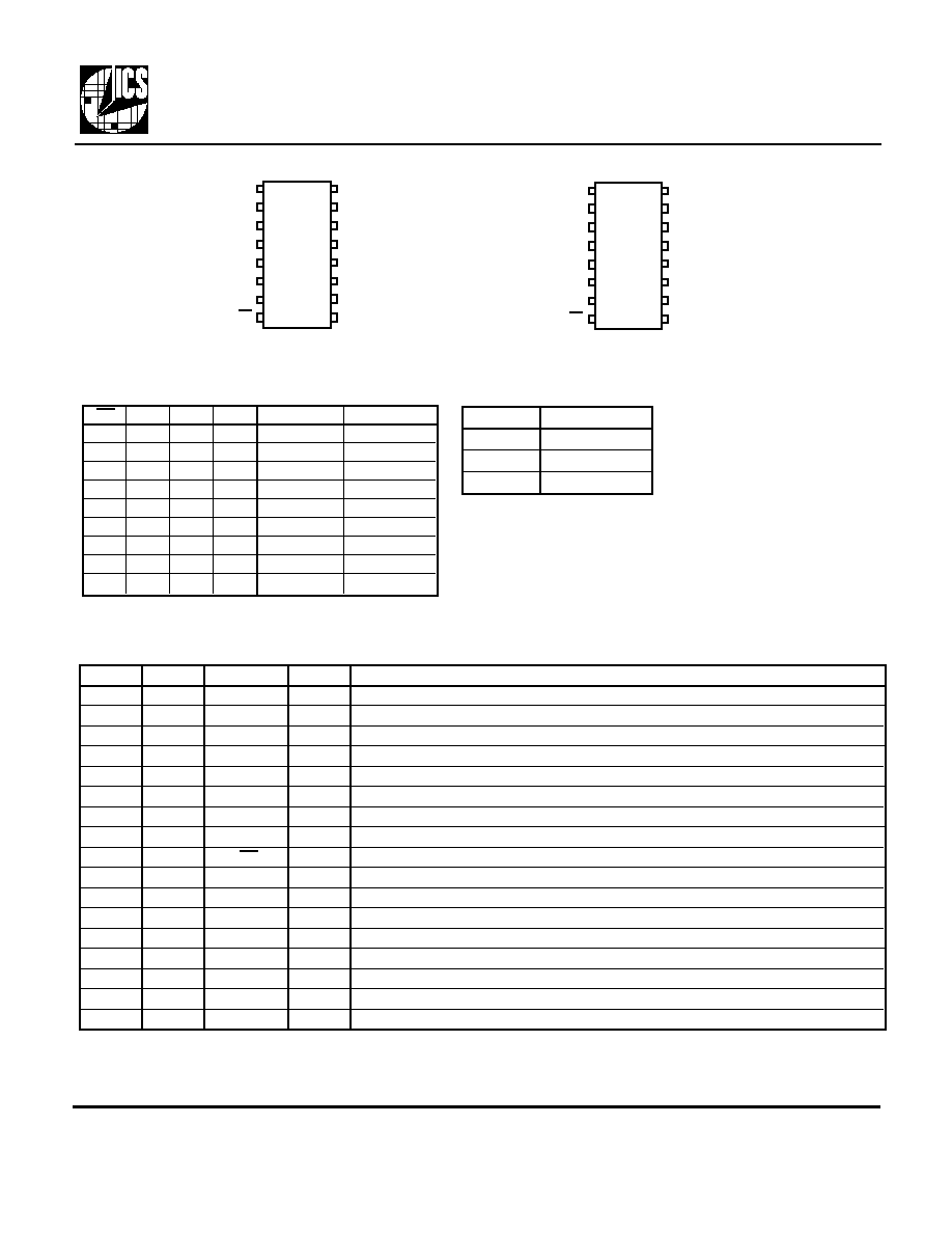
Pin Assignment
1
8
9
16
2
3
4
5
6
7
10
11
12
13
14
15
FS2
X2
24M
BCLK
VDD
GND
X1
PS
FS1
14.3M
CPU
2XCPU
VDD
GND
BCLKS
FS0
BCLKS
BCLK (MHz)
0
25.00
M
33.33
1
50.00
1
8
9
16
2
3
4
5
6
7
10
11
12
13
14
15
FS2
X2
40M
BCLK
VDD
GND
X1
PS
FS1
14.3M
CPU
2XCPU
VDD
GND
BCLKS
FS0
Local Bus Clock Decoding Table (in MHz)
相关PDF资料 |
PDF描述 |
|---|---|
| MK2703SITR | 27 MHz, OTHER CLOCK GENERATOR, PDSO8 |
| MPC8343ZQAGDB | 32-BIT, 400 MHz, MICROPROCESSOR, PBGA620 |
| MPC8347ECVVAJFB | 32-BIT, 533 MHz, MICROPROCESSOR, PBGA672 |
| MPC8347ECVVALDB | 32-BIT, 667 MHz, MICROPROCESSOR, PBGA672 |
| MPC8347EVRAGDB | 32-BIT, 400 MHz, MICROPROCESSOR, PBGA620 |
相关代理商/技术参数 |
参数描述 |
|---|---|
| MK1434STR | 制造商:ICS 制造商全称:ICS 功能描述:Green PC and Local Bus Clock Source |
| MK144 | 制造商:Velleman Inc 功能描述:FLASHING HEART SMD KIT |
| MK1442 | 制造商:ICS 制造商全称:ICS 功能描述:SCSI and Ethernet Clock Source |
| MK1442-01S | 制造商:ICS 制造商全称:ICS 功能描述:SCSI and Ethernet Clock Source |
| MK1442-02S | 制造商:ICS 制造商全称:ICS 功能描述:SCSI and Ethernet Clock Source |
发布紧急采购,3分钟左右您将得到回复。