- 您现在的位置:买卖IC网 > PDF目录65811 > MK2049-45SITR 125 MHz, OTHER CLOCK GENERATOR, PDSO20 PDF资料下载
参数资料
| 型号: | MK2049-45SITR |
| 元件分类: | 时钟产生/分配 |
| 英文描述: | 125 MHz, OTHER CLOCK GENERATOR, PDSO20 |
| 封装: | 0.300 INCH, SOIC-20 |
| 文件页数: | 1/9页 |
| 文件大小: | 185K |
| 代理商: | MK2049-45SITR |
MK2049-45
MDS 2049-45 G
1
Revision 101904
Integrated Circuit Systems, Inc.
● 525 Race Street, San Jose, CA 95126 ● tel (408) 297-1201 ● www.icst.com
3.3V Communications Clock PLL
Description
The MK2049-45 is a dual Phase-Locked Loop (PLL)
device which can provide frequency synthesis and jitter
attenuation. The first PLL is VCXO based and uses a
pullable crystal to track signal wander and attenuate
input jitter. The second PLL is a translator for frequency
multiplication. Basic configuration is determined by a
Mode/Frequency Selection Table. Loop bandwidth and
damping factor are programmable via external loop
filter component selection.
Buffer Mode accepts a 10 to 50MHz input and will
provide a jitter attenuated output at 0.5 x ICLK, 1 x
ICLK or 2 x ICLK. In this mode the MK2049-45 is ideal
for filtering jitter from high frequency clocks.
In External Mode, ICLK accepts an 8 kHz clock and will
produce output frequencies from a table of common
communciations clock rates, CLK and CLK/2. This
allows for the generation of clocks frequency-locked to
an 8 kHz backplane clock, simplifying clock
synchronization in communications systems.
The MK2049-45 can be dynamically switched between
T1, E1, T3, E3 outputs with the same 24.576 MHz
crystal.
ICS can customize these devices for many other
different frequencies. Contact your ICS representative
for more details.
Features
Packaged in 20 pin SOIC
3.3 V + 5% operation
Meets the TR62411, ETS300 011, and GR-1244
specification for MTIE, Pull-in/Hold-in Range, Phase
Transients, and Jitter Generation for Stratum 3, 4,
and 4E
Accepts multiple inputs: 8 kHz backplane clock, or 10
to 50 MHz
Locks to 8 kHz + 100 ppm (External mode)
Buffer Mode allows jitter attenuation of 10 - 50 MHz
input and x1 / x0.5 or x1 / x2 outputs
Exact internal ratios enable zero ppm error
Output rates include T1, E1, T3, E3, and OC3
submultiples
Available in Pb (lead) free package
See also the MK2049-34 and MK2049-36
Not recommended for new designs. Use the
MK2049-45A.
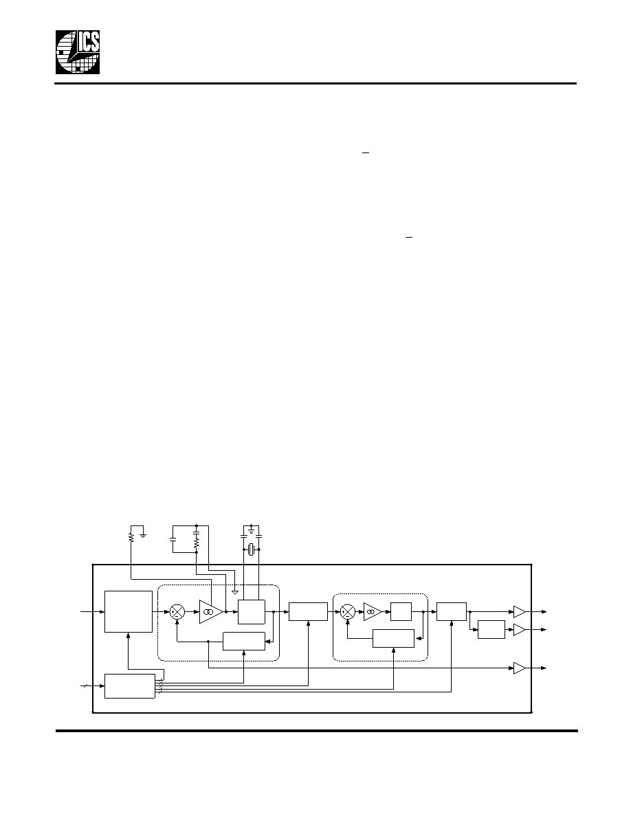
Block Diagram
Charge
Pump
VCXO
X2
X1
ISET
CAP2
Feedback
Divider (N)
Reference
Divider
(used in buffer
mode only)
ICLK
Reference
Divider
Phase
Detector
VCXO
PLL
Feedback
Divider
VCO
Translator
PLL
CLK
CAP1
Output
Divider
Divide
by 2
CLK/2
8k
R
S
R
SET
C
P
C
S
Optional Crystal Load Caps
Divider Value
Look-up Table
FS3:0
4
C
L
C
L
External Pullable Crystal
相关PDF资料 |
PDF描述 |
|---|---|
| MK2049-45SILFTR | 125 MHz, OTHER CLOCK GENERATOR, PDSO20 |
| MK2475-24SLFT | 60 MHz, VIDEO CLOCK GENERATOR, PDSO16 |
| MK2475-24ST | 60 MHz, VIDEO CLOCK GENERATOR, PDSO16 |
| MK2703BS | 27 MHz, OTHER CLOCK GENERATOR, PDSO8 |
| MK2703BSI | 27 MHz, OTHER CLOCK GENERATOR, PDSO8 |
相关代理商/技术参数 |
参数描述 |
|---|---|
| MK205/100G | 制造商:Fischer Elektronik GmbH & Co KG 功能描述:Bulk |
| MK2058-01 | 制造商:ICS 制造商全称:ICS 功能描述:Communications Clock Jitter Attenuator |
| MK205801SI | 制造商:ICS 功能描述: |
| MK2058-01SI | 功能描述:IC VCXO CLK JITTER ATTEN 20-SOIC RoHS:否 类别:集成电路 (IC) >> 时钟/计时 - 时钟发生器,PLL,频率合成器 系列:- 标准包装:39 系列:- 类型:* PLL:带旁路 输入:时钟 输出:时钟 电路数:1 比率 - 输入:输出:1:10 差分 - 输入:输出:是/是 频率 - 最大:170MHz 除法器/乘法器:无/无 电源电压:2.375 V ~ 3.465 V 工作温度:0°C ~ 70°C 安装类型:* 封装/外壳:* 供应商设备封装:* 包装:* |
| MK2058-01SILF | 功能描述:时钟合成器/抖动清除器 COMMUNICATIONS CLOCK JITTER ATTENUATOR RoHS:否 制造商:Skyworks Solutions, Inc. 输出端数量: 输出电平: 最大输出频率: 输入电平: 最大输入频率:6.1 GHz 电源电压-最大:3.3 V 电源电压-最小:2.7 V 封装 / 箱体:TSSOP-28 封装:Reel |
发布紧急采购,3分钟左右您将得到回复。