- 您现在的位置:买卖IC网 > PDF目录45328 > MK2069-02GILFTR 160 MHz, OTHER CLOCK GENERATOR, PDSO56 PDF资料下载
参数资料
| 型号: | MK2069-02GILFTR |
| 元件分类: | 时钟产生/分配 |
| 英文描述: | 160 MHz, OTHER CLOCK GENERATOR, PDSO56 |
| 封装: | 6.10 MM, 0.50 MM PITCH, TSSOP-56 |
| 文件页数: | 2/20页 |
| 文件大小: | 347K |
| 代理商: | MK2069-02GILFTR |
VCXO-Based Clock Jitter Attenuator and Translator
MDS 2069-02 G
10
Revision 050203
Integrated Circuit Systems, Inc. l 525 Race Street, San Jose, CA 95126 l tel (408) 295-9800 l
MK2069-02
CLR Input
When CLR is low, the VCXO PLL charge pump output
is inactivated which means that no charge pump
correction pulses are provided to the loop filter,
therefore the input clock is ignored. During this time,
the VCXO frequency is held constant by the residual
charge or voltage on the PLL loop filter, regardless of
the input clock condition. However, the VCXO
frequency will drift over time, eventually to the minimum
pull range of the crystal, due to leak-off of the loop filter
charge. This means that CLR can provide a holdover
function, but only for a very short duration, typically in
milliseconds. TCLK is always locked to VCLK
regardless of the state of the CLR input.
The Lock Detection circuit is also reset when CLR is
brought low.
In other versions of the MK2069, such as the
MK2069-01, MK2069-02, and MK2069-03, the CLR pin
also provides input phase compensation by resetting
the input divider. This is not the case with the
MK2069-02.
Lock Detection
The MK2069-02 includes a lock detection feature that
indicates lock status of VCLK relative to the selected
input reference clock. When phase lock is achieved
(such as following power-up), the LD output goes high.
When phase lock is lost (such as when the input clock
stops, drifts beyond the pullable range of the crystal, or
suddenly shifts in phase), the LD output goes low.
The definition of a “locked” condition is determined by
the user. LD is high when the VCXO PLL phase
detector error is below the user-defined threshold. This
threshold is set by external components RLD and CLD
shown in the Lock Detection Circuit Diagram, below.
To help guard against false lock indications, the LD pin
will go high only when the phase error is below the set
threshold for 8 consecutive phase detector cycles. The
LD pin will go low when the phase error is above the set
threshold for only 1 phase detector cycle.
The lock detector threshold (phase error) is determined
by the following relationship:
(LD Threshold) = 0.6 x R x C
Where:
1 k
< R < 1 M (to avoid excessive noise or
leakage)
C > 50 pF (to avoid excessive error due to stray
capacitance, which can be as much as 10 pF
including Cin of LDC)
Lock Detector Application example:
The desired maximum allowable loop phase error
for a generated 19.44MHz clock is 100UI which is
5.1
s.
Solution: 5.1
s = (0.001 f) x (8.5 k)
Under ideal conditions, where the VCXO is phase-
locked to a low-jitter reference input, loop phase error is
typically maintained to within a few nanoseconds.
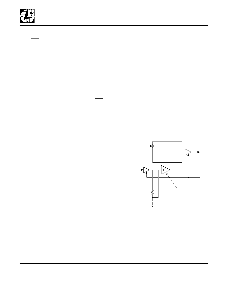
Lock Detection Circuit Diagram
If the lock detection circuit is not used, the LDR output
may remain unconnected, however the LDC input
should be tied high or low. If the PCB was designed to
accommodate the RLD and CLD components but the
LD output will not be used, RLD can remain unstuffed
and CLD can be replaced with a resistor (< 10 kohm).
L o ck D e tectio n C irc u it
Loc k
Q u alificatio n
C o unte r
(8 up, 1 d o w n )
VC XO
Ph a s e
De te c to r
E rro r
Ou tp u t
LD
LD C
LD R
RL D
CL D
RESET
FV
Div id e r
Ou tp u t
OE L
Inpu t Thre s hold
set to V D D /2
相关PDF资料 |
PDF描述 |
|---|---|
| MK2069-02GILFTR | 160 MHz, OTHER CLOCK GENERATOR, PDSO56 |
| MK2069-03GITR | 160 MHz, OTHER CLOCK GENERATOR, PDSO56 |
| MK2069-03GITR | 160 MHz, OTHER CLOCK GENERATOR, PDSO56 |
| MK2069-04GITR | 160 MHz, OTHER CLOCK GENERATOR, PDSO56 |
| MK2069-04GI | 160 MHz, OTHER CLOCK GENERATOR, PDSO56 |
相关代理商/技术参数 |
参数描述 |
|---|---|
| MK2069-03 | 制造商:ICS 制造商全称:ICS 功能描述:VCXO-Based Clock Translator with High Multiplication |
| MK2069-03GI | 功能描述:IC VCXO CLK TRANSLATOR 56-TSSOP RoHS:否 类别:集成电路 (IC) >> 时钟/计时 - 时钟发生器,PLL,频率合成器 系列:- 标准包装:27 系列:Precision Edge® 类型:频率合成器 PLL:是 输入:PECL,晶体 输出:PECL 电路数:1 比率 - 输入:输出:1:1 差分 - 输入:输出:无/是 频率 - 最大:800MHz 除法器/乘法器:是/无 电源电压:3.135 V ~ 5.25 V 工作温度:0°C ~ 85°C 安装类型:表面贴装 封装/外壳:28-SOIC(0.295",7.50mm 宽) 供应商设备封装:28-SOIC 包装:管件 |
| MK2069-03GITR | 功能描述:时钟发生器及支持产品 VCXO-BASED CLOCK TRANSLATOR RoHS:否 制造商:Silicon Labs 类型:Clock Generators 最大输入频率:14.318 MHz 最大输出频率:166 MHz 输出端数量:16 占空比 - 最大:55 % 工作电源电压:3.3 V 工作电源电流:1 mA 最大工作温度:+ 85 C 安装风格:SMD/SMT 封装 / 箱体:QFN-56 |
| MK2069-04 | 制造商:ICS 制造商全称:ICS 功能描述:VCXO-Based Universal Clock Translator |
| MK2069-04GI | 功能描述:IC VCXO CLK TRANSLATOR 56-TSSOP RoHS:否 类别:集成电路 (IC) >> 时钟/计时 - 时钟发生器,PLL,频率合成器 系列:- 标准包装:39 系列:- 类型:* PLL:带旁路 输入:时钟 输出:时钟 电路数:1 比率 - 输入:输出:1:10 差分 - 输入:输出:是/是 频率 - 最大:170MHz 除法器/乘法器:无/无 电源电压:2.375 V ~ 3.465 V 工作温度:0°C ~ 70°C 安装类型:* 封装/外壳:* 供应商设备封装:* 包装:* |
发布紧急采购,3分钟左右您将得到回复。