- 您现在的位置:买卖IC网 > PDF目录45328 > MK2069-02GILFTR (INTEGRATED DEVICE TECHNOLOGY INC) 160 MHz, OTHER CLOCK GENERATOR, PDSO56 PDF资料下载
参数资料
| 型号: | MK2069-02GILFTR |
| 厂商: | INTEGRATED DEVICE TECHNOLOGY INC |
| 元件分类: | 时钟产生/分配 |
| 英文描述: | 160 MHz, OTHER CLOCK GENERATOR, PDSO56 |
| 封装: | 6.10 MM, 0.50 MM PITCH, TSSOP-56 |
| 文件页数: | 14/20页 |
| 文件大小: | 347K |
| 代理商: | MK2069-02GILFTR |
VCXO-Based Clock Jitter Attenuator and Translator
MDS 2069-02 G
3
Revision 050203
Integrated Circuit Systems, Inc. l 525 Race Street, San Jose, CA 95126 l tel (408) 295-9800 l
MK2069-02
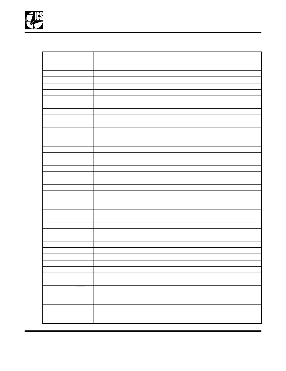
Pin Descriptions
Pin
Number
Pin
Name
Pin
Type
Pin Description
1
PV5
Input
Phase Detector Divider bit 5, VCXO PLL, internal pull-up.
2
PV6
Input
Phase Detector Divider bit 6, VCXO PLL, internal pull-up.
3
PV7
Input
Phase Detector Divider bit 7, VCXO PLL, internal pull-up.
4
PV8
Input
Phase Detector Divider bit 8, VCXO PLL, internal pull-up.
5
FT0
Input
Feedback Divider bit 0 input, Translator PLL, internal pull-up.
6
FT1
Input
Feedback Divider bit 1 input, Translator PLL, internal pull-up.
7
FT2
Input
Feedback Divider bit 2 input, Translator PLL, internal pull-up.
8
PV9
Input
Phase Detector Divider bit 9, VCXO PLL, internal pull-up.
9
PV10
Input
Phase Detector Divider bit 10, VCXO PLL, internal pull-up.
10
PV11
Input
Phase Detector Divider bit 11, VCXO PLL, internal pull-up.
11
ST
Input
Scaling Divider selection bit, Translator PLL, internal pull-up.
12
VDDT
Power
Power Supply connection for translator PLL.
13
GNDT
Ground
Ground connection for translator PLL.
14
X1
-
Crystal oscillator input. Connect this pin to the external reference crystal.
15
VDDV
Power
Power Supply connection for VCXO PLL.
16
X2
-
Crystal oscillator output. Connect this pin to the external reference crystal.
17
GNDV
Ground
Ground connection for VCXO PLL.
18
LFR
-
Loop filter connection, reference node. Refer to loop filter circuit on page 6.
19
LF
-
Loop filter connection, active node. Refer to loop filter circuit on page 6.
20
ISET
-
Charge pump current setting pin. Refer to loop filter circuit on page 6.
21
FV0
Input
Feedback Divider bit 0 input, VCXO PLL, internal pull-up.
22
FV1
Input
Feedback Divider bit 1input, VCXO PLL, internal pull-up.
23
FV2
Input
Feedback Divider bit 2 input, VCXO PLL, internal pull-up.
24
FV3
Input
Feedback Divider bit 3 input, VCXO PLL, internal pull-up.
25
FV4
Input
Feedback Divider bit 4 input, VCXO PLL, internal pull-up.
26
FV5
Input
Feedback Divider bit 5 input, VCXO PLL, internal pull-up.
27
FV6
Input
Feedback Divider bit 6 input, VCXO PLL, internal pull-up.
28
FV7
Input
Feedback Divider bit 7 input, VCXO PLL, internal pull-up.
29
FV8
Input
Feedback Divider bit 8 input, VCXO PLL, internal pull-up.
30
FV9
Input
Feedback Divider bit 9 input, VCXO PLL, internal pull-up.
31
FV10
Input
Feedback Divider bit 10 input, VCXO PLL, internal pull-up.
32
FV11
Input
Feedback Divider bit 11 input, VCXO PLL, internal pull-up.
33
PV0
Input
Phase Detector Divider bit 0, VCXO PLL, internal pull-up.
34
PV1
Input
Phase Detector Divider bit 1, VCXO PLL, internal pull-up.
35
ICLK
Input
Reference clock input, 5V tolerant input.
36
CLR
Input
Clear input, allows VCXO to free-run when low, internal pull-up.
37
LDC
-
Lock detector threshold setting circuit connection. Refer to circuit on page 10.
38
GND
Ground
Digital ground connection.
39
LDR
Power
Lock detector threshold setting circuit connection. Refer to circuit on page 10.
40
RCLK
Output
Reference Clock output, pre-divided phase detector feedback clock.
41
GNDP
Ground
Ground connection for output drivers (VCLK, TCLK, RCLK, LD, LDR).
相关PDF资料 |
PDF描述 |
|---|---|
| MK2069-03GITR | 160 MHz, OTHER CLOCK GENERATOR, PDSO56 |
| MK2069-03GITR | 160 MHz, OTHER CLOCK GENERATOR, PDSO56 |
| MK2069-04GITR | 160 MHz, OTHER CLOCK GENERATOR, PDSO56 |
| MK2069-04GI | 160 MHz, OTHER CLOCK GENERATOR, PDSO56 |
| MK20DN512ZVLL10 | RISC MICROCONTROLLER, PQFP100 |
相关代理商/技术参数 |
参数描述 |
|---|---|
| MK2069-03 | 制造商:ICS 制造商全称:ICS 功能描述:VCXO-Based Clock Translator with High Multiplication |
| MK2069-03GI | 功能描述:IC VCXO CLK TRANSLATOR 56-TSSOP RoHS:否 类别:集成电路 (IC) >> 时钟/计时 - 时钟发生器,PLL,频率合成器 系列:- 标准包装:27 系列:Precision Edge® 类型:频率合成器 PLL:是 输入:PECL,晶体 输出:PECL 电路数:1 比率 - 输入:输出:1:1 差分 - 输入:输出:无/是 频率 - 最大:800MHz 除法器/乘法器:是/无 电源电压:3.135 V ~ 5.25 V 工作温度:0°C ~ 85°C 安装类型:表面贴装 封装/外壳:28-SOIC(0.295",7.50mm 宽) 供应商设备封装:28-SOIC 包装:管件 |
| MK2069-03GITR | 功能描述:时钟发生器及支持产品 VCXO-BASED CLOCK TRANSLATOR RoHS:否 制造商:Silicon Labs 类型:Clock Generators 最大输入频率:14.318 MHz 最大输出频率:166 MHz 输出端数量:16 占空比 - 最大:55 % 工作电源电压:3.3 V 工作电源电流:1 mA 最大工作温度:+ 85 C 安装风格:SMD/SMT 封装 / 箱体:QFN-56 |
| MK2069-04 | 制造商:ICS 制造商全称:ICS 功能描述:VCXO-Based Universal Clock Translator |
| MK2069-04GI | 功能描述:IC VCXO CLK TRANSLATOR 56-TSSOP RoHS:否 类别:集成电路 (IC) >> 时钟/计时 - 时钟发生器,PLL,频率合成器 系列:- 标准包装:39 系列:- 类型:* PLL:带旁路 输入:时钟 输出:时钟 电路数:1 比率 - 输入:输出:1:10 差分 - 输入:输出:是/是 频率 - 最大:170MHz 除法器/乘法器:无/无 电源电压:2.375 V ~ 3.465 V 工作温度:0°C ~ 70°C 安装类型:* 封装/外壳:* 供应商设备封装:* 包装:* |
发布紧急采购,3分钟左右您将得到回复。