- 您现在的位置:买卖IC网 > PDF目录80350 > MK2720SLF 54 MHz, OTHER CLOCK GENERATOR, PDSO8 PDF资料下载
参数资料
| 型号: | MK2720SLF |
| 元件分类: | 时钟产生/分配 |
| 英文描述: | 54 MHz, OTHER CLOCK GENERATOR, PDSO8 |
| 封装: | 0.150 INCH, SOIC-8 |
| 文件页数: | 3/4页 |
| 文件大小: | 58K |
| 代理商: | MK2720SLF |
MK2720
Low Cost 27 + 54 MHz VCXO
MDS 2720 B
3
Revision 031398
Printed 11/16/00
MicroClock Division of ICS1271 Parkmoor Ave.San JoseCA95126(408)295-9800tel(408)295-9818fax
PRELIMINARY INFORMATION
I C R O
C LOC K
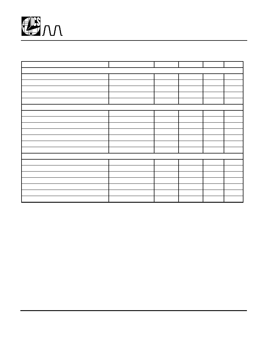
Parameter
Conditions
Minimum
Typical
Maximum
Units
ABSOLUTE MAXIMUM RATINGS (note 1)
Supply voltage, VDD
Referenced to GND
7
V
Inputs and Clock Outputs
Referenced to GND
-0.5
VDD+0.5
V
Ambient Operating Temperature
0
70
°C
Soldering Temperature
Max of 10 seconds
260
°C
Storage temperature
-65
150
°C
DC CHARACTERISTICS (VDD = 5.0V unless noted)
Operating Voltage, VDD
4.75
5.25
V
Output High Voltage, VOH
IOH=-25mA
2.4
V
Output Low Voltage, VOL
IOL=25mA
0.4
V
Output High Voltage, VOH, CMOS level
IOH=-8mA
VDD-0.4
V
Operating Supply Current, IDD
No Load
25
mA
Short Circuit Current
±100
mA
VIN, VCXO control voltage
0
3
V
AC CHARACTERISTICS (VDD = 5.0V unless noted)
Input Crystal Frequency
13.50000
MHz
Input Crystal Accuracy
±30
ppm
Output Clock Rise Time
0.8 to 2.0V
1.5
ns
Output Clock Fall Time
2.0 to 0.8V
1.5
ns
Output Clock Duty Cycle
At 1.4V
45
50
55
%
Maximum Absolute Jitter, short term
200
ps
Output pullability, note 2
0V
≤ VIN ≤ 3V
±100
ppm
Electrical Specifications
Notes:
1. Stresses beyond those listed under Absolute Maximum Ratings could cause permanent damage to the device. Prolonged
exposure to levels above the operating limits but below the Absolute Maximums may affect device reliability.
2. With a MicroClock approved pullable crystal.
External Components
The MK2720 requires a minimum number of external components for proper operation. A decoupling
capacitor of 0.1F should be connected between VDD and GND on pins 2 and 4, as close to the MK2720
as possible. A series termination resistor of 33
may be used for the clock output. The input crystal must be
connected as close to the chip as possible. The input crystal should be a parallel mode, pullable, AT cut,
13.5MHz, with 14pF load capacitance. Consult MicroClock for recommended suppliers. IMPORTANT -
read application note MAN05 before laying out the PCB.
相关PDF资料 |
PDF描述 |
|---|---|
| MC68HSC05P1DW | 8-BIT, MROM, 2.1 MHz, MICROCONTROLLER, PDSO28 |
| MC68010G12D | 16-BIT, 12.5 MHz, MICROPROCESSOR, PDIP64 |
| MC68010L8D | 16-BIT, 8 MHz, MICROPROCESSOR, CDIP64 |
| MDDFMM-TTL-10J | 10 MHz, OTHER CLOCK GENERATOR, PDSO4 |
| MDDFMM-TTL-30F | 30 MHz, OTHER CLOCK GENERATOR, PDIP4 |
相关代理商/技术参数 |
参数描述 |
|---|---|
| MK2722 | 制造商:ICS 制造商全称:ICS 功能描述:Sigma Designs Clock Source |
| MK2722-01S | 制造商:ICS 制造商全称:ICS 功能描述:Sigma Designs Clock Source |
| MK2722-01STR | 制造商:ICS 制造商全称:ICS 功能描述:Sigma Designs Clock Source |
| MK2727 | 制造商:ICS 制造商全称:ICS 功能描述:Low Cost 27 MHz VCXO |
| MK2727S | 功能描述:IC VCXO/PLL CLK SYNTHESIZR 8SOIC RoHS:否 类别:集成电路 (IC) >> 时钟/计时 - 时钟发生器,PLL,频率合成器 系列:- 标准包装:39 系列:- 类型:* PLL:带旁路 输入:时钟 输出:时钟 电路数:1 比率 - 输入:输出:1:10 差分 - 输入:输出:是/是 频率 - 最大:170MHz 除法器/乘法器:无/无 电源电压:2.375 V ~ 3.465 V 工作温度:0°C ~ 70°C 安装类型:* 封装/外壳:* 供应商设备封装:* 包装:* |
发布紧急采购,3分钟左右您将得到回复。