- 您现在的位置:买卖IC网 > PDF目录80516 > MK2731-04STRLF (INTEGRATED DEVICE TECHNOLOGY INC) 36.864 MHz, VIDEO CLOCK GENERATOR, PDSO16 PDF资料下载
参数资料
| 型号: | MK2731-04STRLF |
| 厂商: | INTEGRATED DEVICE TECHNOLOGY INC |
| 元件分类: | 时钟产生/分配 |
| 英文描述: | 36.864 MHz, VIDEO CLOCK GENERATOR, PDSO16 |
| 封装: | 0.150 INCH, SOIC-16 |
| 文件页数: | 2/4页 |
| 文件大小: | 59K |
| 代理商: | MK2731-04STRLF |
MK2731-04C
MPEG Audio Clock
MDS 2731-04 CA
2
Revision 122799
Printed 11/16/00
Integrated Circuit Systems, Inc. 525 Race Street San Jose CA 95126 (408)295-9800tel www.icst.com
PRELIMINARY INFORMATION
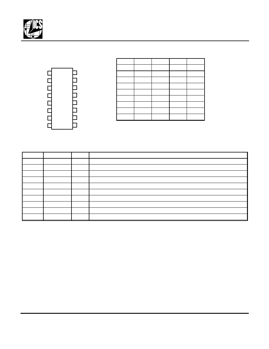
Pin Descriptions
Key: I = Input with internal pull-up resistor; O = output; P = power supply connection; XI, XO = crystal
connections
Pin Assignment
Number
Name
Type
Description
1
X2
XO
Crystal connection. Connect to a parallel mode 14.4 MHz crystal.
2
X1
XI
Crystal connection. Connect to a parallel mode 14.4 MHz crystal.
3, 4, 10
VDD
P
Connect to +3.3V or +5V. Must be same at all VDDs.
5, 6, 7
GND
P
Connect to ground.
8
S2
I
Frequency select pin 2. Determines clock outputs per table above.
9
CLK1
O
Clock output 1 set by status of S0-S2. See table above. This output is CLK2/2
11
CLK2
O
Clock output 2 set by status of S0-S2. See table above.
12, 15, 16
DC
-
Don't Connect. Do not connect anything to these pins.
13
S1
I
Frequency select pin 1. Determines clock outputs per table above.
14
S0
I
Frequency select pin 0. Determines clock outputs per table above.
Key:
0 = connect directly to GND
1 = connect directly to VDD
16
15
14
13
16 pin narrow (150 mil) SOIC
12
11
10
9
1
2
3
4
5
6
7
8
MK2731-04
VDD
GND
X2
X1
VDD
S2
GND
S1
DC
CLK1
CLK2
DC
S0
VDD
S2
S1
S0
CLK1
CLK2
Pin 8
Pin 13
Pin 14
Pin 9
Pin 11
0
16.9344 33.8688
0
1
11.2896 22.5792
0
1
0
8.192
16.384
0
1
18.432
36.864
1
0
11.2896 22.5792
1
0
1
12.288
24.576
1
0
Test
1
Test
Output Clocks Select Table (MHz)
External Components
The MK2731-04 requires a minimum number of external components for proper operation. Decoupling
capacitors of 0.01F should be connected between VDD and GND on pins 3 and 5, and VDD and GND
on pins 10 and 6, as close to the MK2731-04 as possible. Other VDDs can be connected to pin 10. A series
termination resistor of 33
may be used for each clock output. Any unused clock outputs should be left
unconnected (DC, floating). The input crystal must be connected as close to the chip as possible. The input
crystal should be fundamental mode, parallel resonant. For accurate outputs, the crystal should be tuned
with two identical capacitors to ground, as shown on the block diagram. The value of these two crystal caps
should be equal to (CL-6)*2, where CL is the crystal load (or correlation) capacitance.
相关PDF资料 |
PDF描述 |
|---|---|
| MK2744-10STR | 81 MHz, VIDEO CLOCK GENERATOR, PDSO16 |
| MK3732-08RILF | 70.656 MHz, OTHER CLOCK GENERATOR, PDSO20 |
| MK3732-17SLFTR | 49.46 MHz, OTHER CLOCK GENERATOR, PDSO16 |
| MPC5602CF1CLH4 | MICROCONTROLLER, PQFP64 |
| MPC5604BF1CMG6 | MICROCONTROLLER, PBGA208 |
相关代理商/技术参数 |
参数描述 |
|---|---|
| MK2732-05 | 制造商:ICS 制造商全称:ICS 功能描述:Low Phase Noise VCXO+Multiplier |
| MK2732-05S | 制造商:ICS 制造商全称:ICS 功能描述:Low Phase Noise VCXO+Multiplier |
| MK2732-05STR | 制造商:ICS 制造商全称:ICS 功能描述:Low Phase Noise VCXO+Multiplier |
| MK2732-06 | 制造商:ICS 制造商全称:ICS 功能描述:Low Phase Noise VCXO+Multiplier |
| MK2732-06G | 功能描述:IC VCXO/MULTIPLIER 16-TSSOP RoHS:否 类别:集成电路 (IC) >> 时钟/计时 - 时钟发生器,PLL,频率合成器 系列:- 标准包装:39 系列:- 类型:* PLL:带旁路 输入:时钟 输出:时钟 电路数:1 比率 - 输入:输出:1:10 差分 - 输入:输出:是/是 频率 - 最大:170MHz 除法器/乘法器:无/无 电源电压:2.375 V ~ 3.465 V 工作温度:0°C ~ 70°C 安装类型:* 封装/外壳:* 供应商设备封装:* 包装:* |
发布紧急采购,3分钟左右您将得到回复。