- 您现在的位置:买卖IC网 > PDF目录39601 > MK3732-05SITR 108 MHz, OTHER CLOCK GENERATOR, PDSO16 PDF资料下载
参数资料
| 型号: | MK3732-05SITR |
| 元件分类: | 时钟产生/分配 |
| 英文描述: | 108 MHz, OTHER CLOCK GENERATOR, PDSO16 |
| 封装: | 0.150 INCH, SOIC-16 |
| 文件页数: | 2/4页 |
| 文件大小: | 59K |
| 代理商: | MK3732-05SITR |
MK3732-05
Low Phase Noise VCXO+Multiplier
MDS 3732-05 B
2
Revision 101001
Integrated Circuit Systems, Inc. 525 Race Street San Jose CA 95126 (408)295-9800 tel www.icst.com
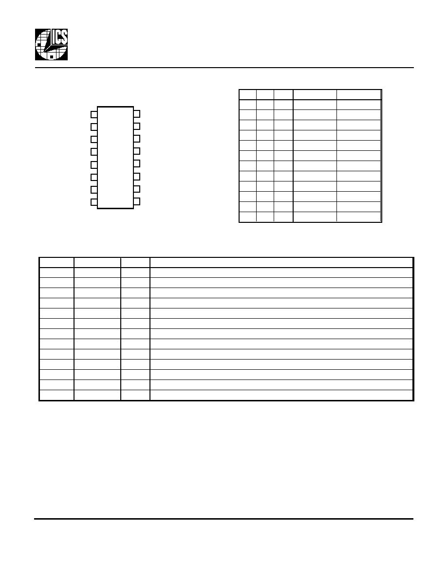
Pin Descriptions
Key: I = Input with internal pull-up resistors; TI = tri-level input; O = output; P = power supply connection; VI = analog
voltage input; XI, XO = crystal pins.
Pin Assignment
Number
Name
Type
Description
1
X1
XI
Crystal connection. Connect to a pullable crystal of 10-18 MHz.
2, 3
VDD
P
Connect to +3.3V.
4
VIN
VI
Voltage Input to VCXO. Zero to 3.3 V signal which controls the frequency of the VCXO.
5, 6, 13
GND
P
Connect to ground.
7
S2
I
Select input pin 2. Selects outputs per table above.
8
OE
I
Output Enable. Tri-states outputs when low.
9
CLK1
O
Clock Output pin 1 per table above.
10
S0
TI
Select input pin 0. Selects outputs per table above.
11
VDD
P
Connect to +3.3V.
12
CLK2
O
Clock Output pin 2 per table above.
14
S1
I
Select input pin 1. Selects outputs per table above.
15
NC
-
Nothing is connected internally to this pin.
16
X2
XO
Crystal connection. Connect to a pullable crystal of 10-18 MHz.
External Components
The MK3732-05 requires a minimum number of external components for proper operation. Decoupling capacitors of
0.01F should be connected between VDD and GND on pins 3 and 5, and VDD and GND on pins 11 and 13, as
close to the MK3732-05 as possible. A series termination resistor of 33
may be used for each clock output. The
input crystal must be connected as close to the chip as possible. The input crystal should be a fundamental mode,
parallel resonant, pullable, AT cut. See page 4 for crystal specifications. Consult ICS for recommended suppliers.
IMPORTANT - consult the application note MAN05 for layout guidelines.
16
15
14
13
16 pin narrow (150 mil) SOIC
12
11
10
9
1
2
3
4
5
6
7
8
VDD
GND
X2
X1
VIN
OE
GND
S2
GND
CLK2
S0
CLK1
VDD
NC
S1
VDD
S2
S1
S0
CLK1
CLK2
0
REF/4
REF/2
0
M
OFF
x0.666
0
1
OFF
x2.6666
0
1
0
OFF
x4
0
1
M
OFF
x1.5
0
1
OFF
x1.3333
1
0
Test
1
0
M
OFF
x4
1
0
1
OFF
x2
1
0
OFF
x3
1
M
OFF
x5
1
OFF
x6
0=connect directly to GND, 1=connect
directly to VDD, OFF=output stopped low.
Clock Select Table
相关PDF资料 |
PDF描述 |
|---|---|
| MK3732-07STR | 49.46 MHz, OTHER CLOCK GENERATOR, PDSO16 |
| MK3732-07SITR | 49.46 MHz, OTHER CLOCK GENERATOR, PDSO16 |
| MK3732-07SI | 49.46 MHz, OTHER CLOCK GENERATOR, PDSO16 |
| MK3754SLF | 54 MHz, OTHER CLOCK GENERATOR, PDSO8 |
| MK3754DLF | 54 MHz, OTHER CLOCK GENERATOR, PDSO8 |
相关代理商/技术参数 |
参数描述 |
|---|---|
| MK3732-07 | 制造商:ICS 制造商全称:ICS 功能描述:ADSL VCXO CLOCK SOURCE |
| MK3732-07S | 制造商:ICS 制造商全称:ICS 功能描述:ADSL VCXO CLOCK SOURCE |
| MK3732-07SI | 制造商:ICS 制造商全称:ICS 功能描述:ADSL VCXO CLOCK SOURCE |
| MK3732-07SITR | 制造商:ICS 制造商全称:ICS 功能描述:ADSL VCXO CLOCK SOURCE |
| MK3732-07STR | 制造商:ICS 制造商全称:ICS 功能描述:ADSL VCXO CLOCK SOURCE |
发布紧急采购,3分钟左右您将得到回复。