- 您现在的位置:买卖IC网 > PDF目录262867 > MK3732-05STR 108 MHz, OTHER CLOCK GENERATOR, PDSO16 PDF资料下载
参数资料
| 型号: | MK3732-05STR |
| 元件分类: | XO, clock |
| 英文描述: | 108 MHz, OTHER CLOCK GENERATOR, PDSO16 |
| 封装: | 0.150 INCH, SOIC-16 |
| 文件页数: | 3/4页 |
| 文件大小: | 59K |
| 代理商: | MK3732-05STR |
MK3732-05
Low Phase Noise VCXO+Multiplier
MDS 3732-05 B
3
Revision 101001
Integrated Circuit Systems, Inc. 525 Race Street San Jose CA 95126 (408)295-9800 tel www.icst.com
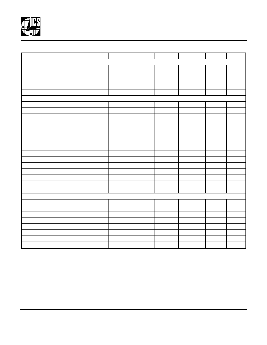
Parameter
Conditions
Minimum
Typical
Maximum
Units
ABSOLUTE MAXIMUM RATINGS (note 1)
Supply voltage, VDD
Referenced to GND
7
V
Inputs and Clock Outputs
Referenced to GND
-0.5
VDD+0.5
V
Ambient Operating Temperature
-40
85
°C
Soldering Temperature
Max of 10 seconds
260
°C
Storage temperature
-65
150
°C
DC CHARACTERISTICS (VDD = 3.3 V unless noted)
Core Operating Voltage, VDD
3.15
3.3
3.45
V
Input High Voltage, VIH, X1 pin only
VDD/2 + 1
VDD/2
V
Input Low Voltage, VIL, X1 pin only
VDD/2
VDD/2 - 1
V
Input High Voltage, VIH, binary inputs
S2, S1, OE
2
V
Input Low Voltage, VIL, binary inputs
S2, S1, OE
0.8
V
Input High Voltage, VIH, trinary input
S0, pin 10
VDD -0.5
V
Input Low Voltage, VIL, trinary input
S0, pin 10
0.5
V
Output High Voltage, VOH
IOH=-12mA
2.4
V
Output Low Voltage, VOL
IOL=12mA
0.4
V
Output High Voltage, VOH, CMOS level
IOH=-8mA
VDD - 0.4
V
Operating Supply Current, IDD
No Load
12
mA
Short Circuit Current
Each output
±50
mA
Input Capacitance
S2:S0, OE
7
pF
Frequency synthesis error
Both clocks
0
ppm
VIN, VCXO control voltage
0
3.3
V
AC CHARACTERISTICS (VDD = 3.3 V unless noted)
Input Crystal Frequency
10
18
MHz
Output Clock Frequency
2.5
108
MHz
Output Clock Rise Time
0.8 to 2.0V
1.5
ns
Output Clock Fall Time
2.0 to 0.8V
1.5
ns
Output Clock Duty Cycle
At VDD/2
40
60
%
Maximum Absolute Jitter
±200
ps
Phase Noise, relative to carrier
10 kHz offset
-115
dBc/Hz
Output pullability, note 2
0V
≤ VIN ≤ 3.3V
±100
ppm
Electrical Specifications
Notes:
1. Stresses beyond those listed under Absolute Maximum Ratings could cause permanent damage to the device.
Prolonged exposure to levels above the operating limits but below the Absolute Maximums may affect device reliability.
2. With an ICS approved pullable crystal.
See application note MAN05 for crystal information. MAN05 is available on the internet at
www.icst.com/pdf/man05.pdf
相关PDF资料 |
PDF描述 |
|---|---|
| M30621MCA-XXXGP | 16-BIT, MROM, 16 MHz, MICROCONTROLLER, PQFP80 |
| M102E1000.0000AK | 1000 MHz, OTHER CLOCK GENERATOR, MDIP24 |
| M41ST84Y-70MH6 | 1 TIMER(S), REAL TIME CLOCK, PDSO28 |
| M48ST59W-70MH6TR | 0 TIMER(S), REAL TIME CLOCK, PDSO44 |
| MB89593BPFV | 8-BIT, MROM, 12 MHz, MICROCONTROLLER, PQFP64 |
相关代理商/技术参数 |
参数描述 |
|---|---|
| MK3732-07 | 制造商:ICS 制造商全称:ICS 功能描述:ADSL VCXO CLOCK SOURCE |
| MK3732-07S | 制造商:ICS 制造商全称:ICS 功能描述:ADSL VCXO CLOCK SOURCE |
| MK3732-07SI | 制造商:ICS 制造商全称:ICS 功能描述:ADSL VCXO CLOCK SOURCE |
| MK3732-07SITR | 制造商:ICS 制造商全称:ICS 功能描述:ADSL VCXO CLOCK SOURCE |
| MK3732-07STR | 制造商:ICS 制造商全称:ICS 功能描述:ADSL VCXO CLOCK SOURCE |
发布紧急采购,3分钟左右您将得到回复。