- 您现在的位置:买卖IC网 > PDF目录9204 > MK5811CMLF (IDT, Integrated Device Technology Inc)IC CLOCK GENERATOR LOW EMI 8SOIC PDF资料下载
参数资料
| 型号: | MK5811CMLF |
| 厂商: | IDT, Integrated Device Technology Inc |
| 文件页数: | 4/10页 |
| 文件大小: | 0K |
| 描述: | IC CLOCK GENERATOR LOW EMI 8SOIC |
| 标准包装: | 97 |
| 类型: | 时钟发生器 |
| PLL: | 是 |
| 输入: | 时钟,晶体 |
| 输出: | LVCMOS |
| 电路数: | 1 |
| 比率 - 输入:输出: | 1:1 |
| 差分 - 输入:输出: | 无/无 |
| 频率 - 最大: | 32MHz |
| 除法器/乘法器: | 无/是 |
| 电源电压: | 3 V ~ 3.63 V |
| 工作温度: | 0°C ~ 85°C |
| 安装类型: | 表面贴装 |
| 封装/外壳: | 8-SOIC(0.154",3.90mm 宽) |
| 供应商设备封装: | 8-SOIC |
| 包装: | 管件 |
| 产品目录页面: | 1254 (CN2011-ZH PDF) |
| 其它名称: | 800-1790 800-1790-5 800-1790-ND |
MK5811C
LOW EMI CLOCK GENERATOR
SSCG
IDT LOW EMI CLOCK GENERATOR
3
MK5811C
REV F 121409
Pin Descriptions
External Components
The MK5811C requires a minimum number of external
components for proper operation.
Decoupling Capacitor
A decoupling capacitor of 0.01F must be connected
between VDD and GND on pins 7 and 2. Connect the
capacitor as close to these pins as possible. For optimum
device performance, mount the decoupling capacitor on the
component side of the PCB. Avoid the use of vias in the
decoupling circuit.
Series Termination Resistor
Use series termination when the PCB trace between the
clock output and the load is over 1 inch. To series terminate
a 50
trace (a commonly used trace impedance), place a
20
resistor in series with the clock line. Place the resistor
as close to the clock output pin as possible. The nominal
impedance of the clock output is 30
.
Tri-level Select Pin Operation
The S1 and S0 select pins are tri-level, meaning that they
have three separate states to make the selections shown in
the table on page 2. To select the M (mid) level, the
connection to these pins must be eliminated by either
floating them originally, or tri-stating the GPIO pins which
drive the select pins.
PCB Layout Recommendations
For optimum device performance and lowest output phase
noise, observe the following guidelines:
1) Mount the 0.01F decoupling capacitor on the
component side of the board as close to the VDD pin as
possible. No vias should be used between the decoupling
capacitor and VDD pin. The PCB trace to the VDD pin and
the PCB trace to the ground via should be kept as short as
possible.
2) To minimize EMI, place the 20
series-termination
resistor (if needed) close to the clock output.
3) An optimum layout is one with all components on the
same side of the board, thus minimizing vias through other
signal layers. Other signal traces should be routed away
from the MK5811C device. This includes signal traces
located underneath the device, or on layers adjacent to the
ground plane layer used by the device.
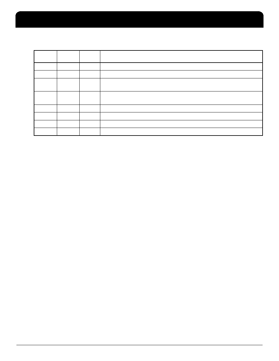
Pin
Number
Pin
Name
Pin Type
Pin Description
1
X1/ICLK
Input
Connect to 4-32 MHz crystal or clock.
2
GND
Power
Connect to ground.
3
S1
Input
Function select 1 input. Selects spread amount and direction per table above.
(default-internal mid-level).
4
S0
Input
Function select 0 input. Selects spread amount and direction per table above.
(default-internal mid-level).
5
SSCLK
Output
Clock output with Spread spectrum
6
FRSEL
Input
Function select for input frequency range. Default to mid level “M”.
7
VDD
Power
Connect to +3.3 V.
8
X2
XO
Crystal connection to 4-32 MHz crystal. Leave unconnected for clock
相关PDF资料 |
PDF描述 |
|---|---|
| VE-B4V-MW-B1 | CONVERTER MOD DC/DC 5.8V 100W |
| D38999/20FG11PN | CONN RCPT 11POS WALL MNT W/PINS |
| VE-B40-MW-B1 | CONVERTER MOD DC/DC 5V 100W |
| MS3106F32-17S | CONN PLUG 4POS STRAIGHT W/SCKT |
| MS3106E32-17S | CONN PLUG 4POS STRAIGHT W/SCKT |
相关代理商/技术参数 |
参数描述 |
|---|---|
| MK5811CMLFT | 功能描述:时钟发生器及支持产品 SPREAD SPECTRUM CLOCK SYNTHESIZER RoHS:否 制造商:Silicon Labs 类型:Clock Generators 最大输入频率:14.318 MHz 最大输出频率:166 MHz 输出端数量:16 占空比 - 最大:55 % 工作电源电压:3.3 V 工作电源电流:1 mA 最大工作温度:+ 85 C 安装风格:SMD/SMT 封装 / 箱体:QFN-56 |
| MK5811G | 制造商:Integrated Device Technology Inc 功能描述:8 TSSOP - Bulk |
| MK5811GLF | 制造商:Integrated Device Technology Inc 功能描述:MK5811GLF - Bulk |
| MK5811GLFTR | 制造商:Integrated Device Technology Inc 功能描述:MK5811GLFTR - Tape and Reel |
| MK5811GTR | 制造商:Integrated Device Technology Inc 功能描述:MK5811GTR - Tape and Reel |
发布紧急采购,3分钟左右您将得到回复。