- 您现在的位置:买卖IC网 > PDF目录80347 > MK74CG117BFIT 100 MHz, OTHER CLOCK GENERATOR, PDSO48 PDF资料下载
参数资料
| 型号: | MK74CG117BFIT |
| 元件分类: | 时钟产生/分配 |
| 英文描述: | 100 MHz, OTHER CLOCK GENERATOR, PDSO48 |
| 封装: | 0.300 INCH, SSOP-48 |
| 文件页数: | 3/7页 |
| 文件大小: | 157K |
| 代理商: | MK74CG117BFIT |
16 Output Low Skew Clock Generator
MDS 74CG117B A
3
Revision 041604
Integrated Circuit Systems, Inc.
525 Race Street, San Jose, CA 95126
tel (408) 297-1201
www.icst.com
MK74CG117B
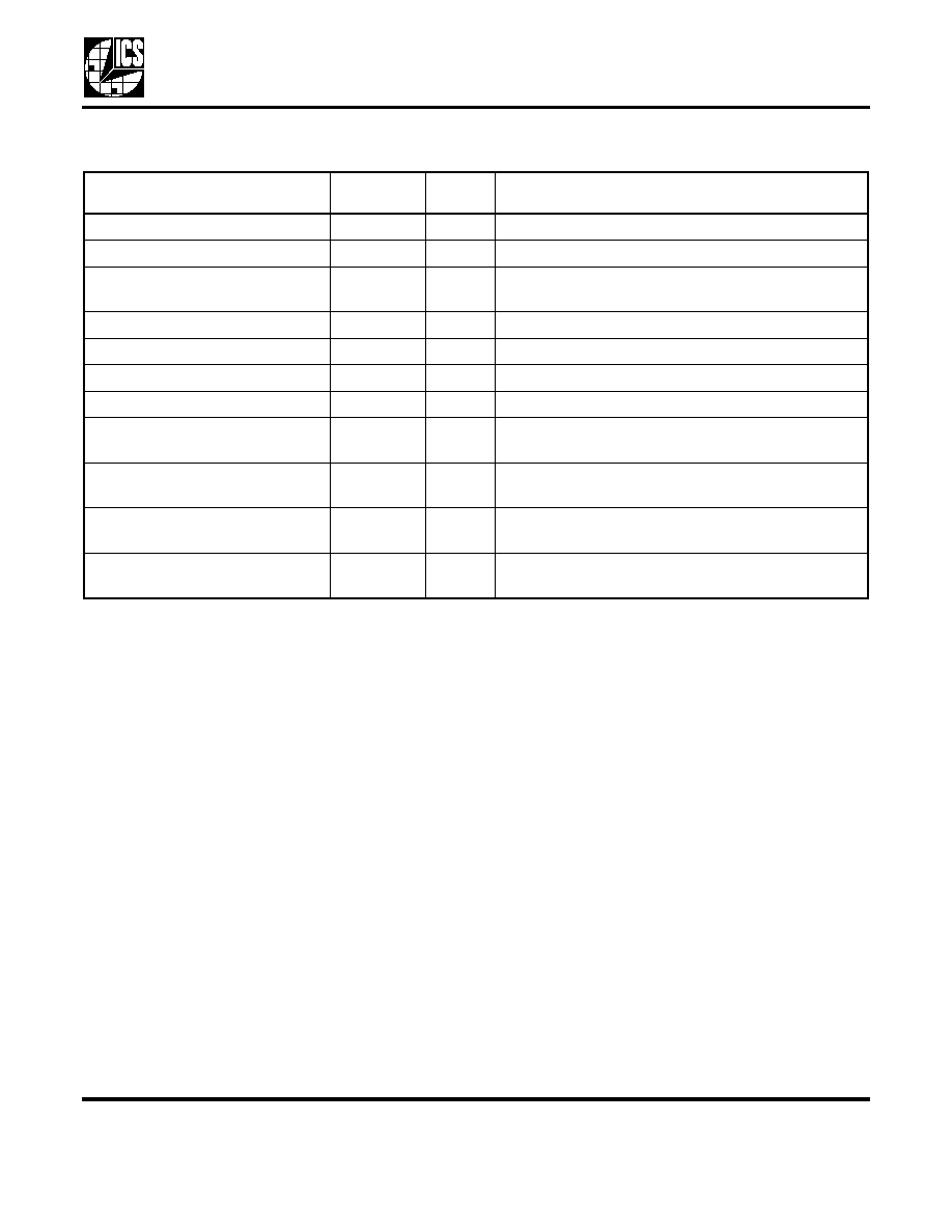
Pin Descriptions
External Components
The MK74CG117B requires a minimum number of
external components for proper operation.
Decoupling Capacitor
A decoupling capacitor of 0.1F must be connected
between each VDD and GND. Connect the capacitor
as close to these pins as possible. For optimum device
performance, mount the decoupling capacitor on the
component side of the PCB. Avoid the use of vias in the
decoupling circuit.
PCB Layout Recommendations
For optimum device performance and lowest output
phase noise, observe the following guidelines:
1) Mount the 0.01F decoupling capacitor on the
component side of the board as close to the VDD pin
as possible. No vias should be used between the
decoupling capacitor and VDD pin. The PCB trace to
the VDD pin and the PCB trace to the ground via
should be kept as short as possible.
2) To minimize EMI, place the 33
series-termination
resistor (if needed) close to the clock output.
3) An optimum layout is one with all components on the
same side of the board, thus minimizing vias through
other signal layers. Other signal traces should be
routed away from the MK74CG117B device. This
includes signal traces located underneath the device,
or on layers adjacent to the ground plane layer used by
the device.
Crystal Information
The crystal used should be a fundamental mode (do
not use third overtone), parallel resonant crystal. The
oscillator has internal caps that provide the proper load
for a crystal with CL = 18 pF. The value of these
capacitors is given by the following equation:
Crystal caps (pF) = (CL - 18) x 2
Pin
Number
Pin
Name
Pin Type
Pin Description
1, 15, 16, 24, 30, 35, 36, 45, 46
VDD
Power
Connect to VDD.
2
X1/ICLK
XI
Connect to a crystal input or clock.
3
X2
XO
Connect to a crystal, or leave unconnected for clock
input.
4, 5, 21, 29, 44
NC
—
No connect. Nothing is connected to these pins.
6, 7, 11, 12, 19, 20, 27, 28, 40, 41
GND
Power
Connect to ground.
8, 10, 48
S2, S1, S0
Input
Multiplier select pins. See table 2.
9
REF
Output
Crystal oscillator buffered reference clock output.
13, 14, 17, 18
CLK1 - 4
Output
Clock 1 - 4. Can be either full or half speed per Table
1.
22, 23, 25, 26, 31, 32, 33, 37
CLK5 - 12
Output
Clock outputs 5 - 12. At full (1x) speed unless
tristated per Table 1.
34, 39
M0, M1
Input
Mode Select pins. Selects tri-state or speed of
outputs per Table 1.
38, 42, 43, 47
CLK13 - 16
Output
Clock 13 - 16. Can be either full or half speed per
Table 1.
相关PDF资料 |
PDF描述 |
|---|---|
| MK1728-01G | 36 MHz, OTHER CLOCK GENERATOR, PDSO8 |
| MC12429FNR2 | 400 MHz, OTHER CLOCK GENERATOR, PQCC28 |
| MK74CG117FILF | 100 MHz, OTHER CLOCK GENERATOR, PDSO48 |
| MK1716R-01RLFT | 133.33 MHz, OTHER CLOCK GENERATOR, PDSO28 |
| MK1726-01ALFTR | 32 MHz, OTHER CLOCK GENERATOR, PDSO8 |
相关代理商/技术参数 |
参数描述 |
|---|---|
| MK74CG117BFLF | 功能描述:时钟发生器及支持产品 16 OUTPUT LOW SKEW CLOCK GENERATOR RoHS:否 制造商:Silicon Labs 类型:Clock Generators 最大输入频率:14.318 MHz 最大输出频率:166 MHz 输出端数量:16 占空比 - 最大:55 % 工作电源电压:3.3 V 工作电源电流:1 mA 最大工作温度:+ 85 C 安装风格:SMD/SMT 封装 / 箱体:QFN-56 |
| MK74CG117BFLFTR | 功能描述:时钟发生器及支持产品 16 OUTPUT LOW SKEW CLOCK GENERATOR RoHS:否 制造商:Silicon Labs 类型:Clock Generators 最大输入频率:14.318 MHz 最大输出频率:166 MHz 输出端数量:16 占空比 - 最大:55 % 工作电源电压:3.3 V 工作电源电流:1 mA 最大工作温度:+ 85 C 安装风格:SMD/SMT 封装 / 箱体:QFN-56 |
| MK74CG117BFTR | 功能描述:IC CLK GEN 16OUTPUT 48-SSOP RoHS:否 类别:集成电路 (IC) >> 时钟/计时 - 时钟发生器,PLL,频率合成器 系列:- 标准包装:39 系列:- 类型:* PLL:带旁路 输入:时钟 输出:时钟 电路数:1 比率 - 输入:输出:1:10 差分 - 输入:输出:是/是 频率 - 最大:170MHz 除法器/乘法器:无/无 电源电压:2.375 V ~ 3.465 V 工作温度:0°C ~ 70°C 安装类型:* 封装/外壳:* 供应商设备封装:* 包装:* |
| MK74ZD133 | 制造商:ICS 制造商全称:ICS 功能描述:PLL and 32-Output Clock Driver |
| MK74ZD133F | 制造商:ICS 制造商全称:ICS 功能描述:PLL and 32-Output Clock Driver |
发布紧急采购,3分钟左右您将得到回复。