- 您现在的位置:买卖IC网 > PDF目录80530 > ML67Q5002TC (OKI ELECTRIC INDUSTRY CO LTD) 32-BIT, FLASH, 60 MHz, RISC MICROCONTROLLER, PQFP144 PDF资料下载
参数资料
| 型号: | ML67Q5002TC |
| 厂商: | OKI ELECTRIC INDUSTRY CO LTD |
| 元件分类: | 微控制器/微处理器 |
| 英文描述: | 32-BIT, FLASH, 60 MHz, RISC MICROCONTROLLER, PQFP144 |
| 封装: | 20 X 20 MM, 0.50 MM PITCH, PLASTIC, LQFP-144 |
| 文件页数: | 6/20页 |
| 文件大小: | 650K |
| 代理商: | ML67Q5002TC |
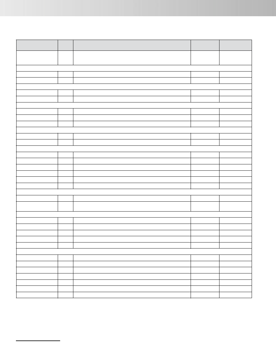
ML675001/ML67Q5002/ML67Q5003
14 Oki Semiconductor
April 2004, Rev 2.0
RI
O
Ring Indicator.
Indicates that the modem or data set has received a telephone ring indicator. Bit 6 in the
modem status register reects this input.
Secondary
Negative
SIO Interface
STXD
O
SIO transmit signal.
Secondary
Positive
SRXD
I
SIO receive signal.
Secondary
Positive
I2C Interface
SDA
I/O
I2C Data. This pin operates as NMOS Open drain. Connect pull-up resistor.
Secondary
—
SCL
O
I2C Clock. This pin operates as NMOS Open drain. Connect pull-up resistor.
Secondary
—
Synchronous SIO Interface
SCLK
I/O
Serial clock.
Secondary
—
SDI
I
Serial receive data.
Secondary
—
SDO
O
Serial transmit data.
Secondary
—
Pulse Width Modulator (PWM) Interface
PWMOUT[0]
O
PWM output of Ch 0.
Secondary
Positive
PWMOUT[1]
O
PWM output of Ch 1.
Secondary
Positive
Analog-to-digital Converter Interface
AIN[0]
I
Ch 0 analog input
—
AIN[1]
I
Ch 1 analog input
—
AIN[2]
I
Ch 2 analog input
—
AIN[3]
I
Ch 3 analog input
—
VREFP
I
Analog-to-digital converter reference voltage
—
VREFN
O
Analog-to-digital converter reference voltage return to ground
—
Interrupt Interface
EXINT[3:0]
I
Interrupt input signals
Secondary
Positive / Negative
EFIQ_N
I
Negative-edge-triggered interrupt input signal. Interrupt controller connects this to CPU FIQ
input
Secondary
Negative
MODE Configuration Interface
DRAME_N
I
DRAM enable mode
—
Negative
TEST
I
Test mode
—Positive
TEST1
I
Test mode
—Positive
FWR
I
Test mode
—Positive
JSEL
I
JTAG select signal: L = On-board debug, H = Boundary scan
—
Power and Ground Interface
AVDD
Analog-to-digital converter power supply, 3.3 V
—
AGND
Analog-to-digital converter ground
—
VDD_CORE
Core power supply, 2.5 V
—
VDD_IO
I/O power supply, 3.3 V
—
GND
GND for core and I/O
—
PLLVDD
PLL power supply, 2.5 V
PLLGND
GND for PLL
Pin Descriptions (Continued)
Pin Name
I/O
Description
Primary/
Secondary
Logic
相关PDF资料 |
PDF描述 |
|---|---|
| MPC8313ECZQAGDA | 32-BIT, 400 MHz, MICROPROCESSOR, PBGA516 |
| MB95F134JBSPFV | 8-BIT, FLASH, 16.25 MHz, MICROCONTROLLER, PDSO30 |
| MC68HC908GZ48VFU | 8-BIT, FLASH, 8 MHz, MICROCONTROLLER, PQFP64 |
| M37510E6FS | 8-BIT, UVPROM, 4 MHz, MICROCONTROLLER, CQCC160 |
| M30280M4V-XXXHP | 16-BIT, MROM, 20 MHz, MICROCONTROLLER, PQFP64 |
相关代理商/技术参数 |
参数描述 |
|---|---|
| ML67Q5003 | 制造商:OKI 制造商全称:OKI electronic componets 功能描述:32-bit ARM-Based General-Purpose Microcontroller |
| ML67Q5003ALA | 制造商:ROHM Semiconductor 功能描述: |
| ML67Q5003LA | 制造商:ROHM Semiconductor 功能描述: |
| ML67Q5003-NNNLA | 制造商:ROHM Semiconductor 功能描述: |
| ML67Q5003-NNNTC | 制造商:ROHM Semiconductor 功能描述: |
发布紧急采购,3分钟左右您将得到回复。