- 您现在的位置:买卖IC网 > PDF目录45333 > ML9041A-01ACVWA (LAPIS SEMICONDUCTOR CO LTD) 17 X 100 DOTS DOT MAT LCD DRVR AND DSPL CTLR, UUC189 PDF资料下载
参数资料
| 型号: | ML9041A-01ACVWA |
| 厂商: | LAPIS SEMICONDUCTOR CO LTD |
| 元件分类: | 显示控制器 |
| 英文描述: | 17 X 100 DOTS DOT MAT LCD DRVR AND DSPL CTLR, UUC189 |
| 封装: | 10.62 X 2.55 MM, GOLD BUMP, DIE-189 |
| 文件页数: | 6/64页 |
| 文件大小: | 653K |
| 代理商: | ML9041A-01ACVWA |
第1页第2页第3页第4页第5页当前第6页第7页第8页第9页第10页第11页第12页第13页第14页第15页第16页第17页第18页第19页第20页第21页第22页第23页第24页第25页第26页第27页第28页第29页第30页第31页第32页第33页第34页第35页第36页第37页第38页第39页第40页第41页第42页第43页第44页第45页第46页第47页第48页第49页第50页第51页第52页第53页第54页第55页第56页第57页第58页第59页第60页第61页第62页第63页第64页
PEDL9041A-02
OKI Semiconductor
ML9041A-xxA/xxB
14/64
FUNCTIONAL DESCRIPTION
Instruction Register (IR), Data Register (DR), and Expansion Instruction Register (ER)
These registers are selected by setting the level of the Register Selection input pins RS
0 and RS1.
The DR is
selected when both RS
0 and RS1 are “H”. The IR is selected when RS0 is “L” and RS1 is “H”. The ER is selected
when both RS
0 and RS1 are “L”. (When RS0 is “H” and RS1 is “L”, the ML9041A is not selected.)
The IR stores an instruction code and sets the address code of the display data RAM (DDRAM) or the character
generator RAM (CGRAM).
The microcontroller (CPU) can write to the IR but cannot read from the IR.
The ER stores a contrast adjusting code and sets the address code of the arbitrator RAM (ABRAM).
The CPU can write to or read from the ER.
The DR stores data to be written in the DDRAM, ABRAM and CGRAM and also stores data read from the
DDRAM, ABRAM and CGRAM.
The data written in the DR by the CPU is automatically written in the DDRAM, ABRAM or CGRAM.
When an address code is written in the IR or ER, the data of the specified address is automatically transferred from
the DDRAM, ABRAM or CGRAM to the DR. The data of the DDRAM, ABRAM and CGRAM can be checked
by allowing the CPU to read the data stored in the DR.
After the CPU writes data in the DR, the data of the next address in the DDRAM, ABRAM or CGRAM is selected
to be ready for the next writing by the CPU. Similarly, after the CPU reads the data in the DR, the data of the next
address in the DDRAM, ABRAM or CGRAM is set in the DR to be ready for the next reading by the CPU.
Writing in or reading from these 3 registers is controlled by changing the status of the R/
W (Read/Write) pin.
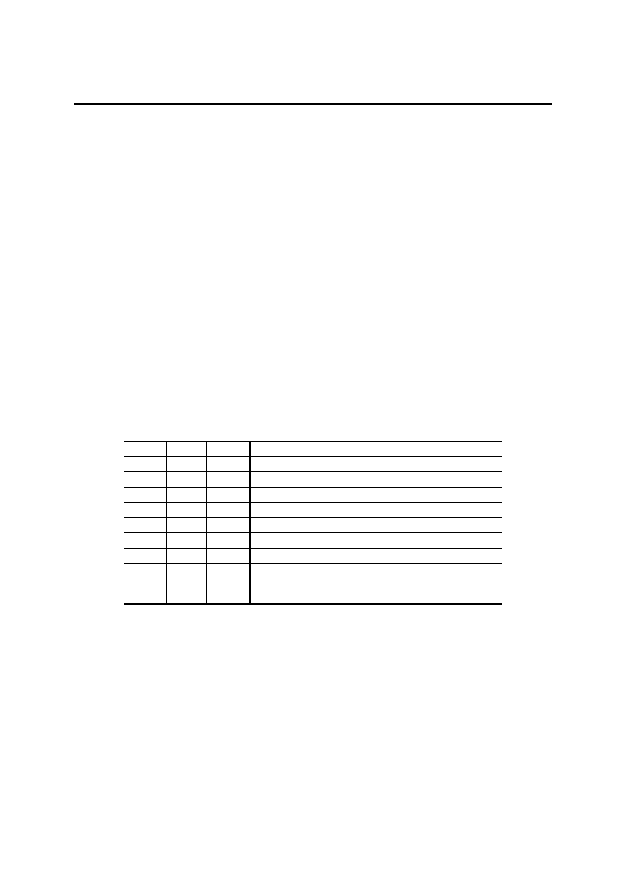
Table 1 R/
W
W pin status and register operation
R/W
RS
0
RS
1
Operation
L
H
Writing in the IR
H
L
H
Reading the Busy flag (BF) and the address counter (ADC)
L
H
Writing in the DR
H
Reading from the DR
L
Writing in the ER
H
L
Reading the contrast code
L
H
L
Disabled (Not in a busy state, not performing the writes)
HH
L
Disabled (Not in a busy state, not performing the reads.
Note data read by the CPU is undefined since the data bus
is high impedance.)
Busy Flag (BF)
The status “1” of the Busy Flag (BF) indicates that the ML9041A is carrying out internal operation.
When the BF is “1”, any new instruction is ignored.
When R/
W = “H”, RS
0 = “L” and RS1 = “H”, the data in the BF is output to the DB7.
New instructions should be input when the BF is “0”.
When the BF is “1”, the output code of the address counter (ADC) is undefined.
相关PDF资料 |
PDF描述 |
|---|---|
| ML9041A-01ACVWA | 17 X 100 DOTS DOT MAT LCD DRVR AND DSPL CTLR, UUC189 |
| ML9041A-XXBCVWA | 17 X 100 DOTS DOT MAT LCD DRVR AND DSPL CTLR, UUC175 |
| ML9042-01DVWA | 17 X 100 DOTS DOT MAT LCD DRVR AND DSPL CTLR, UUC233 |
| ML9042-01CVWA | 17 X 100 DOTS DOT MAT LCD DRVR AND DSPL CTLR, UUC233 |
| ML9042-01DVWA | 17 X 100 DOTS DOT MAT LCD DRVR AND DSPL CTLR, UUC233 |
相关代理商/技术参数 |
参数描述 |
|---|---|
| ML9041A-XXACVWA | 制造商:OKI 制造商全称:OKI electronic componets 功能描述:DOT MATRIX LCD CONTROLLER DRIVER |
| ML9041A-XXBCVWA | 制造商:OKI 制造商全称:OKI electronic componets 功能描述:DOT MATRIX LCD CONTROLLER DRIVER |
| ML9042 | 制造商:OKI 制造商全称:OKI electronic componets 功能描述:DOT MATRIX LCD CONTROLLER DRIVER |
| ML9042-54CVWA-5016 | 制造商:ROHM Semiconductor 功能描述:RHOML9042-54CVWA-5016 OKI LCD DRIVER |
| ML9044 | 制造商:OKI 制造商全称:OKI electronic componets 功能描述:DOT MATRIX LCD CONTROLLER DRIVER |
发布紧急采购,3分钟左右您将得到回复。