- 您现在的位置:买卖IC网 > PDF目录45333 > ML9206-XXGS-K (OKI ELECTRIC INDUSTRY CO LTD) 16 X 37 DOTS FLUORESCENT DSPL CTRL, PDSO64 PDF资料下载
参数资料
| 型号: | ML9206-XXGS-K |
| 厂商: | OKI ELECTRIC INDUSTRY CO LTD |
| 元件分类: | 显示控制器 |
| 英文描述: | 16 X 37 DOTS FLUORESCENT DSPL CTRL, PDSO64 |
| 封装: | 0.525 INCH, 0.80 MM PITCH, PLASTIC, SSOP-64 |
| 文件页数: | 7/33页 |
| 文件大小: | 356K |
| 代理商: | ML9206-XXGS-K |
第1页第2页第3页第4页第5页第6页当前第7页第8页第9页第10页第11页第12页第13页第14页第15页第16页第17页第18页第19页第20页第21页第22页第23页第24页第25页第26页第27页第28页第29页第30页第31页第32页第33页
Semiconductor
ML9206-xx
15/32
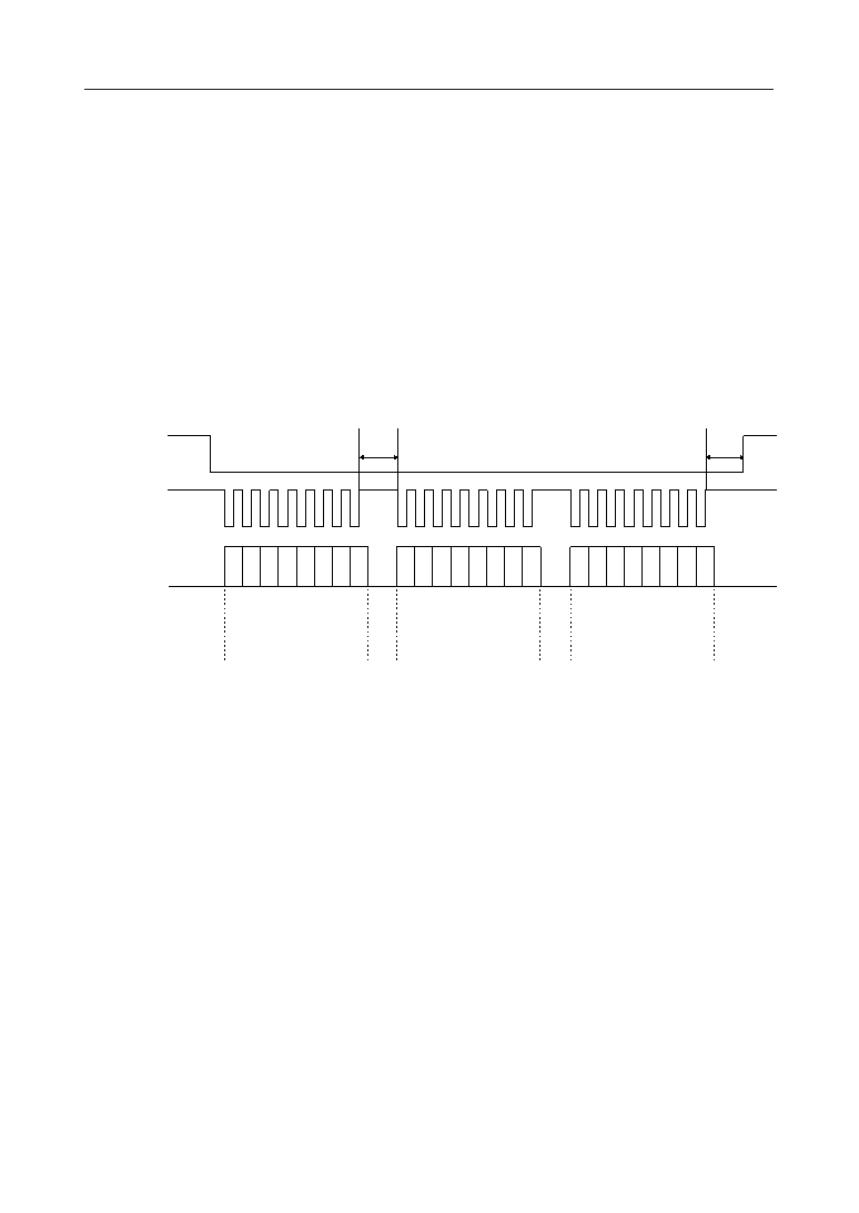
Data Transfer Method and Command Write Method
Display control command and data are written by an 8-bit serial transfer.
Write timing is shown in the figure below.
Setting the CS pin to "Low" level enables a data transfer.
Data is 8 bits and is sequentially input into the DA pin from LSB (LSB first).
As shown in the figure below, data is read by the shift register at the rising edge of the shift clock,
which is input into the CP pin. If 8-bit data is input, internal load signals are automatically
generated and data is written to each register and RAM.
Therefore it is not necessary to input load signals from the outside.
Setting the CS pin to "High" disables data transfer. Data input from the point when the CS pin
changes from "High" to "Low" is recognized in 8-bit units.
*
When data is written to RAM (DCRAM, ADRAM, CGRAM) continuously, addresses are
internally incremented automatically.
Therefore it is not necessary to specify the 1st byte to write RAM data for the 2nd and later
bytes.
Reset Function
Reset is executed when the RESET pin is set to "L", (when turning power on, for example) and
initializes all functions.
Initial status is as follows.
Address of each RAM .................. address "00"H
Data of each RAM ........................ All contents are undefined
General output port ..................... All general output ports go "Low"
Display digit .................................. 16 digits
Brightness adjustment ................. 0/256
All display lights ON or OFF ..... OFF mode
Segment output ............................ All segment outputs go "Low"
AD output ..................................... All AD outputs go "Low"
Please set again according to "Setting Flowchart" after reset.
tDOFF
B0
LSB
CS
CP
DA
B1 B2 B3 B4 B5 B6 B7
B0 B1 B2 B3 B4 B5 B6 B7
MSB
1st byte
LSB
MSB
2nd byte
When data is written to DCRAM* Command and address data
tCSH
B0 B1 B2 B3 B4 B5 B6 B7
LSB
MSB
2nd byte
Character code data of the
next address
Character code data
相关PDF资料 |
PDF描述 |
|---|---|
| ML9206-XXMB | 36 X 16 DOTS DOT MAT LCD DRVR AND DSPL CTLR, PDSO64 |
| ML9206-XXGA | 36 X 16 DOTS DOT MAT LCD DRVR AND DSPL CTLR, PQFP64 |
| ML9207-01GP | 24 X 36 DOTS FLUORESCENT DSPL CTRL, PQFP80 |
| ML9207-XXGA | 24 X 36 DOTS FLUORESCENT DSPL CTRL, PQFP80 |
| ML9207-01GA | 24 X 36 DOTS FLUORESCENT DSPL CTRL, PQFP80 |
相关代理商/技术参数 |
参数描述 |
|---|---|
| ML9207 | 制造商:OKI 制造商全称:OKI electronic componets 功能描述:5 X 7 Dot Character × 24-Digit Display Controller/Driver with Character RAM |
| ML9207-XX | 制造商:OKI 制造商全称:OKI electronic componets 功能描述:5 X 7 Dot Character × 24-Digit Display Controller/Driver with Character RAM |
| ML9207-XXGA | 制造商:OKI 制造商全称:OKI electronic componets 功能描述:5 X 7 Dot Character 】 24-Digit Display Controller/Driver with Character RAM |
| ML9207-XXGP | 制造商:OKI 制造商全称:OKI electronic componets 功能描述:5 X 7 Dot Character × 24-Digit Display Controller/Driver with Character RAM |
| ML9208 | 制造商:OKI 制造商全称:OKI electronic componets 功能描述:5 X 7 Dot Character X 16-Digit Display Controller/Driver with Character RAM |
发布紧急采购,3分钟左右您将得到回复。