- 您现在的位置:买卖IC网 > PDF目录382331 > MM54C74 (National Semiconductor Corporation) Dual D Flip-Flop PDF资料下载
参数资料
| 型号: | MM54C74 |
| 厂商: | National Semiconductor Corporation |
| 英文描述: | Dual D Flip-Flop |
| 中文描述: | 双D触发器 |
| 文件页数: | 1/6页 |
| 文件大小: | 120K |
| 代理商: | MM54C74 |
TL/F/5885
M
February 1988
MM54C74/MM74C74 Dual D Flip-Flop
General Description
The MM54C74/MM74C74 dual D flip-flop is a monolithic
complementary MOS (CMOS) integrated circuit constructed
with N- and P-channel enhancement transistors. Each flip-
flop has independent data, preset, clear and clock inputs
and Q and Q outputs. The logic level present at the data
input is transferred to the output during the positive going
transition of the clock pulse. Preset or clear is independent
of the clock and accomplished by a low level at the preset
or clear input.
Features
Y
Supply voltage range
3V to 15V
Y
Tenth power TTL compatible
Drive 2 LPT
2
L loads
0.45 V
CC
(typ.)
Y
High noise immunity
Y
Low power
50 nW (typ.)
10 MHz (typ.)
with 10V supply
Y
Medium speed operation
Applications
Y
Automotive
Y
Data terminals
Y
Instrumentation
Y
Medical electronics
Y
Alarm system
Y
Industrial electronics
Y
Remote metering
Y
Computers
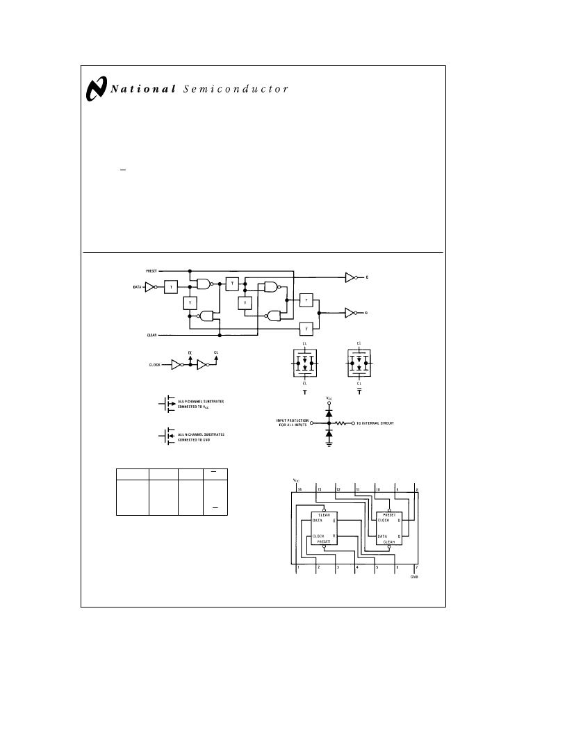
Logic Diagram
TL/F/5885–1
Truth Table
Preset
Clear
Q
n
Q
n
0
0
1
1
0
1
0
1
0
1
0
0
0
1
*
Q
n
*
Q
n
*
No change in output from previous state.
Order Number MM54C74 or MM74C74
Connection Diagram
Dual-In-Line Package
TL/F/5885–2
Top View
Note: A logic ‘‘0’’ on clear sets Q to logic ‘‘0’’.
A logic ‘‘0’’ on preset sets Q to logic ‘‘1’’.
C
1995 National Semiconductor Corporation
RRD-B30M105/Printed in U. S. A.
相关PDF资料 |
PDF描述 |
|---|---|
| MM54C74J | Dual D Flip-Flop |
| MM54C74N | Dual D Flip-Flop |
| MM54C85 | 4-Bit Magnitude Comparator |
| MM54C85J | 4-Bit Magnitude Comparator |
| MM54C85N | 4-Bit Magnitude Comparator |
相关代理商/技术参数 |
参数描述 |
|---|---|
| MM54C74J | 制造商:NSC 制造商全称:National Semiconductor 功能描述:Dual D Flip-Flop |
| MM54C74J883C | 制造商:NATIONAL 功能描述:* |
| MM54C74N | 制造商:NSC 制造商全称:National Semiconductor 功能描述:Dual D Flip-Flop |
| MM54C74W/883 | 制造商:Rochester Electronics LLC 功能描述:- Bulk |
| MM54C76 WAF | 制造商:Texas Instruments 功能描述: |
发布紧急采购,3分钟左右您将得到回复。