- 您现在的位置:买卖IC网 > PDF目录382335 > MM74C918N (NATIONAL SEMICONDUCTOR CORP) Dual CMOS 30V Relay Driver PDF资料下载
参数资料
| 型号: | MM74C918N |
| 厂商: | NATIONAL SEMICONDUCTOR CORP |
| 元件分类: | 外设及接口 |
| 英文描述: | Dual CMOS 30V Relay Driver |
| 中文描述: | 0.5 A 2 CHANNEL, NAND GATE BASED PRPHL DRVR, PDIP14 |
| 封装: | PLASTIC, DIP-14 |
| 文件页数: | 2/6页 |
| 文件大小: | 153K |
| 代理商: | MM74C918N |
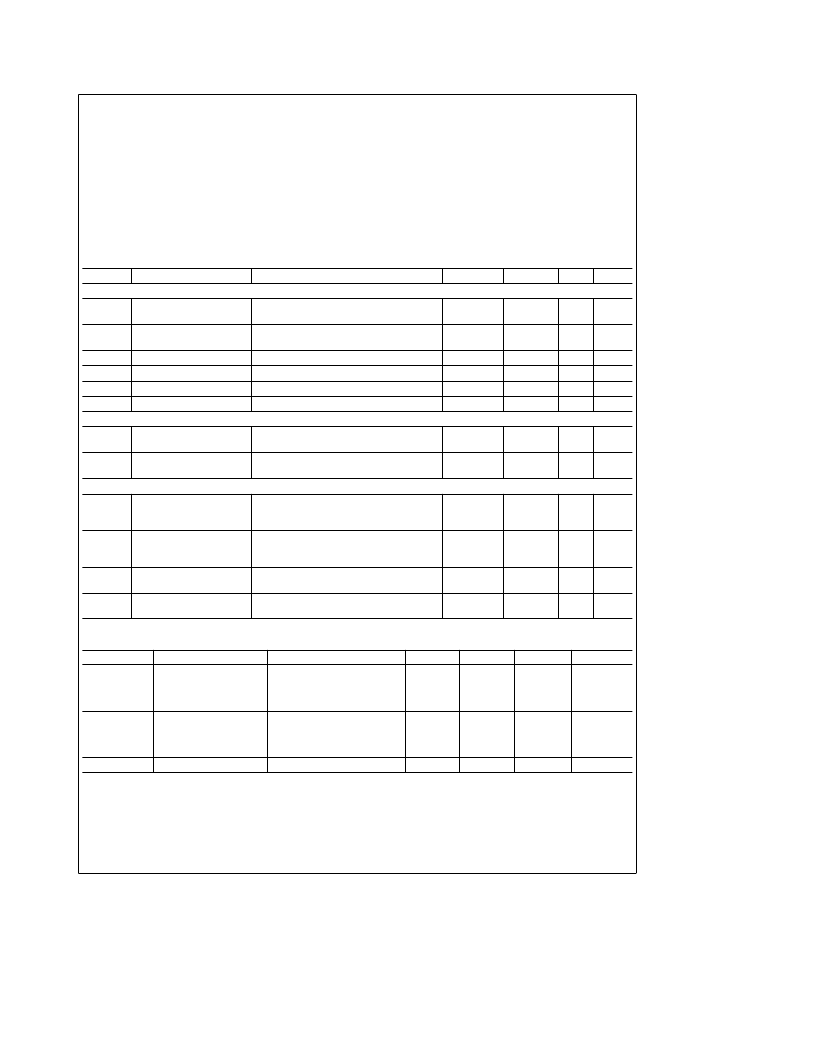
Absolute Maximum Ratings
(Note 1)
If Military/Aerospace specified devices are required,
please contact the National Semiconductor Sales
Office/Distributors for availability and specifications.
Voltage at any Input Pin
b
0.3V to V
CC
a
0.3V
Voltage at any Output Pin
32V
Operating Temperature Range
MM74C908/MM74C918
b
40
§
C to
a
85
§
C
Operating V
CC
Range
Absolute Maximum V
CC
I
SOURCE
Storage Temperature Range (T
S
)
Lead Temperature (T
L
)
(Soldering, 10 seconds)
4V to 18V
19V
500 mA
b
65
§
C to
a
150
§
C
260
§
C
Power Dissipation (P
D
)
Refer to Maximum Power
Dissipation vs Ambient
Temperature Graph
DC Electrical Characteristics
Min/Max limits apply across temperature range, unless otherwise noted
Symbol
Parameter
Conditions
Min
Typ
Max
Units
CMOS TO CMOS
V
IN(1)
Logical ‘‘1’’ Input Voltage
V
CC
e
5V
V
CC
e
10V
V
CC
e
5V
V
CC
e
10V
V
CC
e
15V, V
IN
e
15V
V
CC
e
15V, V
IN
e
0V
V
CC
e
15V, Outputs Open Circuit
V
IN
e
V
CC
, I
OUT
e b
200
m
A
3.5
8.0
V
V
V
IN(0)
Logical ‘‘0’’ Input Voltage
1.5
2.0
V
V
I
IN(1)
I
IN(0)
I
CC
Logical ‘‘1’’ Input Current
0.005
1.0
m
A
Logical ‘‘0’’ Input Current
b
1.0
b
0.005
m
A
Supply Current
0.05
15
m
A
Output ‘‘OFF’’ Voltage
b
30
V
CMOS/LPTTL INTERFACE
V
IN(1)
Logical ‘‘1’’ Input Voltage
MM74C908/MM74C918
V
CC
e
4.75V
V
CC
b
1.5
V
V
IN(0)
Logical ‘‘0’’ Input Voltage
MM74C908/MM74C918
V
CC
e
4.75V
0.8
V
OUTPUT DRIVE
V
OUT
Output Voltage
I
OUT
e b
300 mA, V
CC
t
5V, T
J
e
25
§
C
I
OUT
e b
250 mA, V
CC
t
5V, T
J
e
65
§
C
I
OUT
e b
175 mA, V
CC
t
5V, T
J
e
150
§
C
I
OUT
e b
300 mA, V
CC
t
5V, T
J
e
25
§
C
I
OUT
e b
250 mA, V
CC
t
5V, T
J
e
65
§
C
I
OUT
e b
175 mA, V
CC
t
5V, T
J
e
150
§
C
V
CC
b
2.7
V
CC
b
3.0
V
CC
b
3.15
V
CC
b
1.8
V
CC
b
1.9
V
CC
b
2.0
6.0
7.5
10
V
V
V
R
ON
Output Resistance
9.0
12
18
X
X
X
Output Resistance
Coefficient
0.55
0.80
%/
§
C
i
JA
Thermal Resistance
MM74C908/MM74C918
(Note 3)
(Note 3)
100
45
110
55
§
C/W
§
C/W
AC Electrical Characteristics
*
Symbol
Parameter
Conditions
Min
Typ
Max
Units
t
pd1
Propagation Delay
to a Logical ‘‘1’’
V
CC
e
5V, R
L
e
50
X
,
C
L
e
50 pF, T
A
e
25
§
C
V
CC
e
10V, R
L
e
50
X
,
C
L
e
50 pF, T
A
e
25
§
C
V
CC
e
5V, R
L
e
50
X
,
C
L
e
50 pF, T
A
e
25
§
C
V
CC
e
10V, R
L
e
50
X
,
C
L
e
50 pF, T
A
e
25
§
C
(Note 2)
150
300
ns
65
120
ns
t
pd0
Propagation Delay
to a Logic ‘‘0’’
2.0
10
m
s
4.0
20
m
s
C
IN
*
AC Parameters are guaranteed by DC correlated testing.
Input Capacitance
5.0
pF
Note 1:
‘‘Absolute Maximum Ratings’’ are those values beyond which the safety of the device cannot be guaranteed. Except for ‘‘Operating Temperature Range’’
they are not meant to imply that the devices should be operated at these limits. The table of ‘‘Electrical Characteristics’’ provides conditions for actual device
operation.
Note 2:
Capacitance is guaranteed by periodic testing.
Note 3:
i
JA
measured in free air with device soldered into printed circuit board.
2
相关PDF资料 |
PDF描述 |
|---|---|
| MM74C928 | 4-Digit Counters with Multiplexed 7-Segment Output Drivers |
| MM74C95 | 4-Bit Right-Shift Left-Shift Register |
| MM74C95J | 4-Bit Right-Shift Left-Shift Register |
| MM74C95N | 4-Bit Right-Shift Left-Shift Register |
| MM54C95 | 4-Bit Right-Shift Left-Shift Register |
相关代理商/技术参数 |
参数描述 |
|---|---|
| MM74C922 | 制造商:NSC 制造商全称:National Semiconductor 功能描述:16, 20-Key Encoder |
| MM74C922N | 功能描述:编码器、解码器、复用器和解复用器 16-Key Encoder RoHS:否 制造商:Micrel 产品:Multiplexers 逻辑系列:CMOS 位数: 线路数量(输入/输出):2 / 12 传播延迟时间:350 ps, 400 ps 电源电压-最大:2.625 V, 3.6 V 电源电压-最小:2.375 V, 3 V 最大工作温度:+ 85 C 安装风格:SMD/SMT 封装 / 箱体:QFN-44 封装:Tray |
| MM74C922N | 制造商:Fairchild Semiconductor Corporation 功能描述:IC 74C CMOS 74C922 DIP18 |
| MM74C922N_Q | 功能描述:编码器、解码器、复用器和解复用器 16-Key Encoder RoHS:否 制造商:Micrel 产品:Multiplexers 逻辑系列:CMOS 位数: 线路数量(输入/输出):2 / 12 传播延迟时间:350 ps, 400 ps 电源电压-最大:2.625 V, 3.6 V 电源电压-最小:2.375 V, 3 V 最大工作温度:+ 85 C 安装风格:SMD/SMT 封装 / 箱体:QFN-44 封装:Tray |
| MM74C922N-G | 制造商:Rochester Electronics LLC 功能描述: |
发布紧急采购,3分钟左右您将得到回复。