- 您现在的位置:买卖IC网 > PDF目录80551 > MM908E626AVPEK (FREESCALE SEMICONDUCTOR INC) FLASH, 32 MHz, MICROCONTROLLER, PDSO54 PDF资料下载
参数资料
| 型号: | MM908E626AVPEK |
| 厂商: | FREESCALE SEMICONDUCTOR INC |
| 元件分类: | 微控制器/微处理器 |
| 英文描述: | FLASH, 32 MHz, MICROCONTROLLER, PDSO54 |
| 封装: | 5.10 X 10.30 MM, 0.65 MM PITCH, LEAD FREE, SOIC-54 |
| 文件页数: | 33/43页 |
| 文件大小: | 842K |
| 代理商: | MM908E626AVPEK |
第1页第2页第3页第4页第5页第6页第7页第8页第9页第10页第11页第12页第13页第14页第15页第16页第17页第18页第19页第20页第21页第22页第23页第24页第25页第26页第27页第28页第29页第30页第31页第32页当前第33页第34页第35页第36页第37页第38页第39页第40页第41页第42页第43页
Analog Integrated Circuit Device Data
Freescale Semiconductor
39
908E626
ADDITIONAL DOCUMENTATION
THERMAL ADDENDUM (REV 1.0)
ADDITIONAL DOCUMENTATION
THERMAL ADDENDUM (REV 1.0)
Introduction
This thermal addendum ia provided as a supplement to the MM908E626
technical data sheet. The addendum provides thermal performance information
that may be critical in the design and development of system applications. All
electrical, application and packaging information is provided in the data sheet.
Package and Thermal Considerations
This MM908E626 is a dual die package. There are two heat sources in the
package independently heating with P1 and P2. This results in two junction
temperatures, TJ1 and TJ2, and a thermal resistance matrix with RJAmn.
For m, n = 1, RJA11 is the thermal resistance from Junction 1 to the reference
temperature while only heat source 1 is heating with P1.
For m = 1, n = 2, RJA12 is the thermal resistance from Junction 1 to the
reference temperature while heat source 2 is heating with P2. This applies to
RJ21 and RJ22, respectively.
The stated values are solely for a thermal performance comparison of one
package to another in a standardized environment. This methodology is not meant to and will not predict the performance of a
package in an application-specific environment. Stated values were obtained by measurement and simulation according to the
standards listed below.
Standards
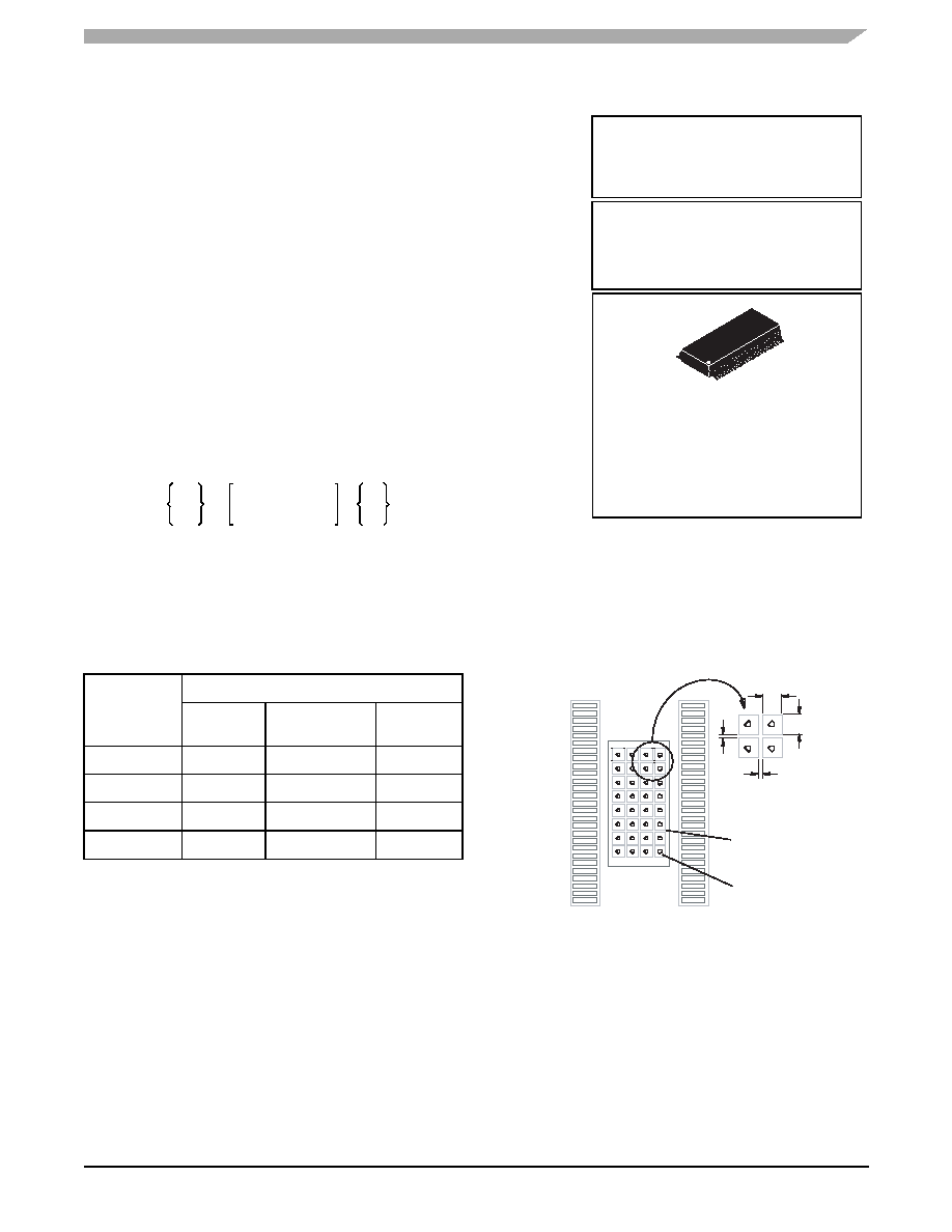
Figure 20. Thermal Land Pattern for Direct Thermal
Attachment Per JEDEC JESD51-5Thermal Test Board
54-PIN
SOICW-EP
908E626
98ARL10519D
54-PIN SOICW-EP
Note For package dimensions, refer to the
908E626 device datasheet.
TJ1
TJ2
=
RJA11
RJA21
RJA12
RJA22
.
P1
P2
Table 12. Thermal Performance Comparison
Thermal
Resistance
1 = Power Chip, 2 = Logic Chip
[
C/W]
m = 1,
n = 1
m = 1, n = 2
m = 2, n = 1
m = 2,
n = 2
RJAmn
23
20
24
RJBmn
9.0
6.0
10
RJAmn
52
47
52
RJCmn (5)
1.0
0
2.0
Notes:
1.
Per JEDEC JESD51-2 at natural convection, still air
condition.
2.
2s2p thermal test board per JEDEC JESD51-7and
JESD51-5.
3.
Per JEDEC JESD51-8, with the board temperature on the
center trace near the power outputs.
4.
Single layer thermal test board per JEDEC JESD51-3 and
JESD51-5.
5.
Thermal resistance between the die junction and the
exposed pad, “infinite” heat sink attached to exposed pad.
1.0
0.2
Soldermast
openings
Thermal vias
connected to top
buried plane
54 Terminal SOIC-EP
0.65 mm Pitch
17.9 mm x 7.5 mm Body
10.3 mm x 5.1 mm Exposed Pad
* All measurements
are in millimeters
相关PDF资料 |
PDF描述 |
|---|---|
| M38062E6FS | 8-BIT, UVPROM, 8 MHz, MICROCONTROLLER, CQCC80 |
| MSM6408-GS-K | 4-BIT, MROM, MICROCONTROLLER, PQFP44 |
| MSM65P544-GS-1K | 8-BIT, OTPROM, 10 MHz, MICROCONTROLLER, PQFP64 |
| MSM80C48-RS | 8-BIT, MROM, 11 MHz, MICROCONTROLLER, PDIP40 |
| MAF8032AH-2-15WP | 8-BIT, 15 MHz, MICROCONTROLLER, PQCC44 |
相关代理商/技术参数 |
参数描述 |
|---|---|
| MM908E626AVPEKR2 | 功能描述:8位微控制器 -MCU RoHS:否 制造商:Silicon Labs 核心:8051 处理器系列:C8051F39x 数据总线宽度:8 bit 最大时钟频率:50 MHz 程序存储器大小:16 KB 数据 RAM 大小:1 KB 片上 ADC:Yes 工作电源电压:1.8 V to 3.6 V 工作温度范围:- 40 C to + 105 C 封装 / 箱体:QFN-20 安装风格:SMD/SMT |
| MM908E626R2 | 制造商:FREESCALE 制造商全称:Freescale Semiconductor, Inc 功能描述:Integrated Stepper Motor Driver with Embedded MCU and LIN Serial Communication |
| MM-90N | 功能描述:ANT MAGN MNT VEHIC 3.5"DIA 10'NF RoHS:是 类别:RF/IF 和 RFID >> RF 天线 系列:* 标准包装:1 系列:* |
| MM90R9F | 制造商:Ohmite Mfg Co 功能描述: |
| MM912_634 | 制造商:FREESCALE 制造商全称:Freescale Semiconductor, Inc 功能描述:Integrated S12 Based Relay Driver with LIN |
发布紧急采购,3分钟左右您将得到回复。