- 您现在的位置:买卖IC网 > Datasheet目录344 > MORPH-IC-II (FTDI, Future Technology Devices International Ltd)MODULE USB TO FPGA Datasheet资料下载
参数资料
| 型号: | MORPH-IC-II |
| 厂商: | FTDI, Future Technology Devices International Ltd |
| 文件页数: | 6/30页 |
| 文件大小: | 0K |
| 描述: | MODULE USB TO FPGA |
| 产品目录绘图: | MORPH-IC-II |
| 特色产品: | USB Hi-Speed FPGA Development Module with Altera Cyclone-II FPGA |
| 标准包装: | 5 |
| 类型: | FPGA |
| 所含物品: | 板 |
| 其它名称: | 768-1097 |
第1页第2页第3页第4页第5页当前第6页第7页第8页第9页第10页第11页第12页第13页第14页第15页第16页第17页第18页第19页第20页第21页第22页第23页第24页第25页第26页第27页第28页第29页第30页
�� ��
��
��`�
�Document� Reference� No.:� FT_000198�
�MORPH-IC-II� Datasheet�
�Version� 1.04�
�Clearance� No.:� FTDI#� 164�
�3�
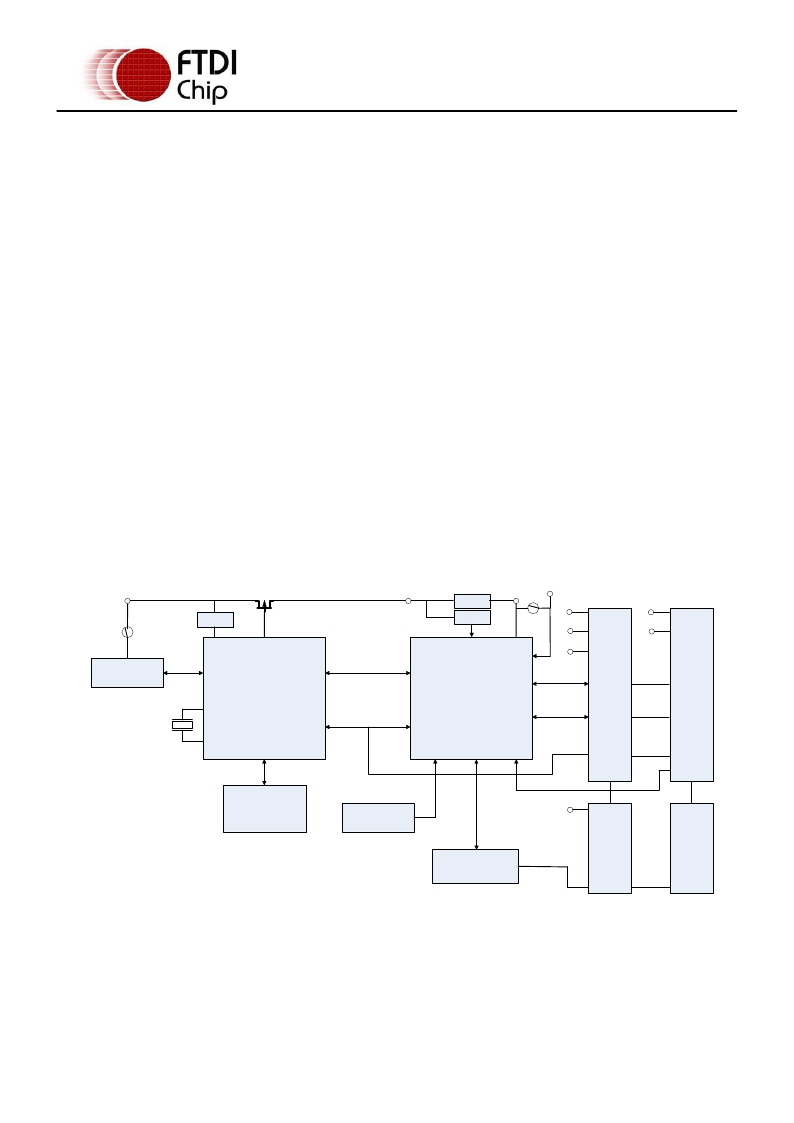
�Functional� Description�
�3.1� Morph-IC-II� Block� Diagram�
�A� block� diagram� of� the� Morph-IC-II� is� given� in� Fig.� 2.� Morph-IC-II� module� can� be� USB� powered� or� self�
�powered.� The� power� mode� is� selected� using� the� “VBUS”� jumper� -� as� indicated� on� the� diagram� below.� The�
�FPGA� can� be� programmed� from� a� PC� via� the� USB� interface� and� the� FT2232H� USB� bridge.�
�FT2232H� requires� a� 12MHz� crystal� and� an� external� EEPROM� which� is� used� to� configure� FT2232H.�
�The� Altera� FPGA� is� powered� from� a� +3.3V� regulator� supply� with� the� exception� of� its� internal� PLLs� which�
�are� powered� by� a� +1.2V� regulated� supply.� The� power� supply� to� the� FPGA� is� disabled,� using� the� MOSFET�
�switch,� when� FT2232H� is� in� power� save� mode.�
�The� I/Os� of� the� FPGA� are� partitioned� into� 4� I/O� banks.� These� banks� each� have� their� own� power�
�connection.� The� voltage� of� the� power� connection� to� each� bank� defines� the� voltage� level� of� the� signals� of�
�that� bank.�
�The� power� supply� to� I/O� bank� 4� is� configured� differently� to� add� more� flexibility.� The� I/O� bank� 4� power�
�can� be� supplied� from� an� external� supply� to� the� V_Bank� 4� pins� on� J2� or� from� the� 3V3IO� net� connected� to�
�the� on� board� regulator.� This� feature� allows� signals� of� different� voltage� levels� to� be� used� in� an� application�
�and� is� explained� with� more� detail� in� Section� 3.2.�
�Morph-IC-II� uses� a� 50MHz� oscillator� which� provides� the� clock� source� to� the� FPGA.� Alternatively� the� FPGA�
�can� be� synchronised� to� an� external� clock� using� the� CLKIN� pin� on� connector� J2.�
�The� four� connectors� J1,� J2,� J3� and� J4� provide� I/O� connectivity� between� Morph-IC-II� and� any� application�
�board.� The� connector� give� a� total� of� 80� signal� lines,� a� FIFO� interface� capability,� power� supply� pins,� an�
�external� clock� line� and� an� external� reset� line.� The� JTAG� interface� can� be� accessed� through� the� JTAG� port�
�or� J3� and� J4� connectors,� using� an� Altera� Byte� Blaster� (or� equivalent)� cable� and� SignalTap� Analyser� which�
�is� an� application� of� Quartus� II� the� signals� of� all� the� I/Os� of� the� FPGA� can� be� displayed� on� a� PC� monitor.�
�VCCUSB�
�MOSFET� POWER� SWTICH�
�3.3V� REG�
�VCCSW�
�3.3V� REG�
�1.2V� REG�
�3V3IO�
�V_Bank4�
�VCCUSB�
�1�
�IO� CONNECTORS�
�29� 30�
�V_Bank4�
�VBUS�
�JUMPER�
�VCC3V3�
�1.2DV�
�VCCSW�
�2�
�3V3IO�
�17� 18�
�17� 18�
�USB�
�USB�
�data�
�PROGRAMMING�
�INTERFACE�
�V_BANK4�
�3V3IO�
�29� 30�
�CONNECTOR�
�FT2232H�
�USB� INTERFACE�
�IC�
�DATA�
�TRANSFER�
�INTERFACE�
�ALTERA�
�CYCLONE� TWO�
�EP2C5F256C8N�
�FPGA�
�BANK4_IO�
�IO�
�J1�
�BANK4_IO�
�IO�
�J2�
�12MHz� XTAL�
�INT�
�CLOCK�
�EXT�
�CLOCK�
�14�
�93C56� USB�
�IO�
�IO�
�CONFIGURATION�
�EEPROM�
�50MHz�
�OSCILLATOR�
�3V3IO�
�12�
�J3�
�J4�
�JTAG�
�PORT�
�JTAG�
�Fig.� 2� –� Hardware� Representation� of� the� Morph-IC-II�
�Copyright� ?� 2010� Future� Technology� Devices� International� Limited�
�5�
�相关PDF资料 |
PDF描述 |
|---|---|
| MP-14000 | ADAPTR QUICKWRTR PIC14000 28-PIN |
| MP-SOIC18 | ADAPTER QUICKWRITER 18-SOIC |
| MP-SSOP18 | ADAPTER QUICKWRITER 18-SSOP |
| MP-ZIF14 | ADAPTER QUICKWRITER 14-PIN ZIF |
| MP-ZIF18/28 | ADAPTER QUICKWRITER 18/28PIN ZIF |
相关代理商/技术参数 |
参数描述 |
|---|---|
| MORPHIC-RB | 功能描述:界面模块 From FTDI Morph-IC Retail Box w/ Softw RoHS:否 制造商:4D Systems 产品:Serial Converters 通道/端口数量: 数据速率: 接口类型:USB, UART 工作电源电压:3.3 V, 5 V 最大工作温度: |
| MORS1W | 制造商:ABCO 制造商全称:ABCO 功能描述:FIXED METAL OXIDE FILM RESISTORS |
| MORS2W | 制造商:ABCO 制造商全称:ABCO 功能描述:FIXED METAL OXIDE FILM RESISTORS |
| MORS3W | 制造商:ABCO 制造商全称:ABCO 功能描述:FIXED METAL OXIDE FILM RESISTORS |
| MORTAR-44LB | 制造商:3M Electronic Products Division 功能描述:3M(TM) FIRE BARRIER MORTAR, 44 98040056073 制造商:3M Electronic Products Division 功能描述:Fire Barrier 44 lb Bag |
发布紧急采购,3分钟左右您将得到回复。