- 您现在的位置:买卖IC网 > PDF目录296598 > MP1484EN-LF-Z (MONOLITHIC POWER SYSTEMS INC) 5.3 A SWITCHING REGULATOR, 380 kHz SWITCHING FREQ-MAX, PDSO8 PDF资料下载
参数资料
| 型号: | MP1484EN-LF-Z |
| 厂商: | MONOLITHIC POWER SYSTEMS INC |
| 元件分类: | 稳压器 |
| 英文描述: | 5.3 A SWITCHING REGULATOR, 380 kHz SWITCHING FREQ-MAX, PDSO8 |
| 封装: | LEAD FREE, MS-012BA, SOIC-8 |
| 文件页数: | 9/10页 |
| 文件大小: | 243K |
| 代理商: | MP1484EN-LF-Z |
MP1484 – 3A, 18V, 340KHz SYNCHRONOUS RECTIFIED STEP-DOWN CONVERTER
MP1484 Rev. 0.1
www.MonolithicPower.com
8
12/14/2007
MPS Proprietary Information. Unauthorized Photocopy and Duplication Prohibited.
2007 MPS. All Rights Reserved.
The system has one zero of importance, due to the
compensation capacitor (C3) and the compensation
resistor (R3). This zero is located at:
3
R
3
C
2
1
f 1
Z
×
π
=
The system may have another zero of
importance, if the output capacitor has a large
capacitance and/or a high ESR value. The zero,
due to the ESR and capacitance of the output
capacitor, is located at:
ESR
R
2
C
2
1
f
×
π
=
In this case, a third pole set by the
compensation
capacitor
(C6)
and
the
compensation
resistor
(R3)
is
used
to
compensate the effect of the ESR zero on the
loop gain. This pole is located at:
3
R
6
C
2
1
f 3
P
×
π
=
The goal of compensation design is to shape
the converter transfer function to get a desired
loop gain. The system crossover frequency
where the feedback loop has the unity gain is
important. Lower crossover frequencies result
in slower line and load transient responses,
while higher crossover frequencies could cause
system instability. A good standard is to set the
crossover frequency below one-tenth of the
switching frequency.
To optimize the compensation components, the
following procedure can be used.
1. Choose the compensation resistor (R3) to set
the desired crossover frequency.
Determine R3 by the following equation:
FB
OUT
CS
EA
S
FB
OUT
CS
EA
C
V
G
f
1
.
0
2
C
2
V
G
f
2
C
2
3
R
×
π
<
×
π
=
Where fC is the desired crossover frequency
which is typically below one tenth of the
switching frequency.
2. Choose the compensation capacitor (C3) to
achieve
the
desired
phase
margin.
For
applications with typical inductor values, setting
the compensation zero (fZ1) below one-forth of
the crossover frequency provides sufficient
phase margin.
Determine C3 by the following equation:
C
f
3
R
2
4
3
C
×
π
>
Where R3 is the compensation resistor.
3. Determine if the second compensation
capacitor (C6) is required. It is required if the
ESR zero of the output capacitor is located at
less than half of the switching frequency, or the
following relationship is valid:
2
f
R
2
C
2
1
S
ESR
<
×
π
If this is the case, then add the second
compensation capacitor (C6) to set the pole fP3
at the location of the ESR zero. Determine C6
by the equation:
3
R
2
C
6
C
ESR
×
=
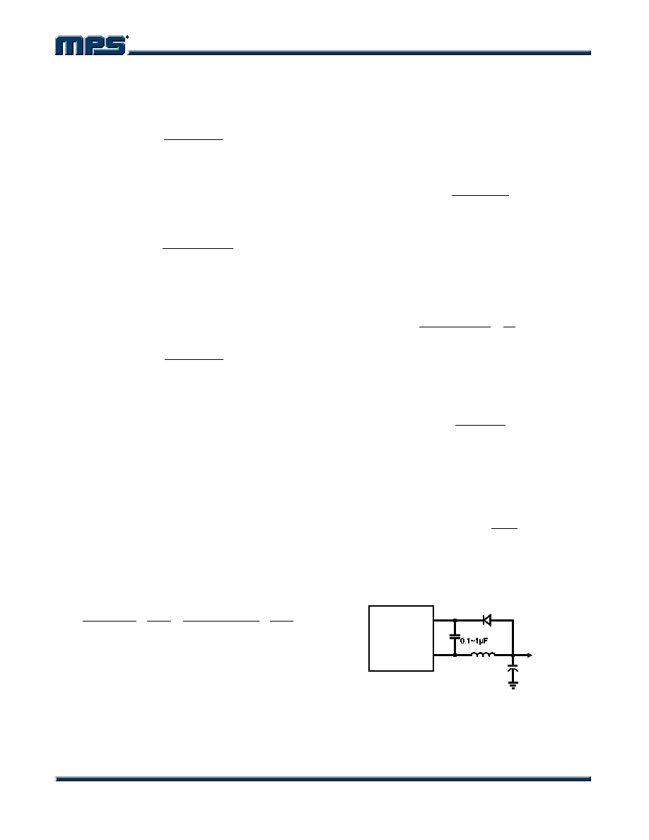
External Bootstrap Diode
An external bootstrap diode may enhance the
efficiency of the regulator, the applicable
conditions of external BS diode are:
VOUT is 5V or 3.3V; and
Duty cycle is high: D=
IN
OUT
V
>65%
In these cases, an external BS diode is
recommended from the output of the voltage
regulator to BS pin, as shown in Fig.2
MP1484
SW
BS
C
L
BST
C
5V or 3.3V
OUT
External BST Diode
IN4148
Figure 2—Add Optional External Bootstrap
Diode to Enhance Efficiency
The recommended external BS diode is IN4148,
and the BS cap is 0.1~1F.
相关PDF资料 |
PDF描述 |
|---|---|
| MP152W | |
| MP1505W | |
| MP156W | |
| MP1510W | |
| MP154W | |
相关代理商/技术参数 |
参数描述 |
|---|---|
| MP1492 | 制造商:MPS 制造商全称:Monolithic Power Systems 功能描述:2A, 4.2V-16V Input, Fast Transient Synchronous Step-down Converter |
| MP1492DS | 制造商:MPS 制造商全称:Monolithic Power Systems 功能描述:2A, 4.2V-16V Input, Fast Transient Synchronous Step-down Converter |
| MP1492DS-A | 制造商:MPS 制造商全称:Monolithic Power Systems 功能描述:2A, 4.2V-16V Input, Fast Transient Synchronous Step-down Converter |
| MP1492DS-A-LF | 功能描述:直流/直流开关转换器 MP1492DS-A-LF RoHS:否 制造商:STMicroelectronics 最大输入电压:4.5 V 开关频率:1.5 MHz 输出电压:4.6 V 输出电流:250 mA 输出端数量:2 最大工作温度:+ 85 C 安装风格:SMD/SMT |
| MP1492DS-A-LF-Z | 功能描述:直流/直流开关转换器 MP1492DS-A-LF-Z RoHS:否 制造商:STMicroelectronics 最大输入电压:4.5 V 开关频率:1.5 MHz 输出电压:4.6 V 输出电流:250 mA 输出端数量:2 最大工作温度:+ 85 C 安装风格:SMD/SMT |
发布紧急采购,3分钟左右您将得到回复。