- 您现在的位置:买卖IC网 > PDF目录385630 > MP230 (Apex Microtechnology Corporation) POWER OPERATIONAL AMPLIFIER PDF资料下载
参数资料
| 型号: | MP230 |
| 厂商: | Apex Microtechnology Corporation |
| 元件分类: | 运动控制电子 |
| 英文描述: | POWER OPERATIONAL AMPLIFIER |
| 中文描述: | 功率运算放大器 |
| 文件页数: | 4/5页 |
| 文件大小: | 309K |
| 代理商: | MP230 |
APEX MICROTECHNOLOGY CORPORATION 5980 NORTH SHANNON ROAD TUCSON, ARIZONA 85741 USA APPLICATIONS HOTLINE: 1 (800) 546-2739
4
OPERATING
CONSIDERATIONS
MP230
GENERAL
Please read Application Note 1 “General Operating Consid-
erations” which covers stability, power supplies, heat sinking,
mounting, current limit, SOA interpretation, and specification
interpretation. Visit www.apexmicrotech.com for design tools
that help automate tasks such as calculations for stability,
internal power dissipation, current limit, heat sink selection,
Apex’s complete Application Notes library, Technical Seminar
Workbook and Evaluation Kits.
GROUND PINS
The MP230 has two ground pins (pins 2, 40). These pins
provide a return for the internal capacitive bypassing of the
small signal stages of the MP230. The two ground pins are not
connected together on the substrate. Both of these pins are
required to be connected to the system signal ground.
BALANCING RESISTOR SELECTION (R
S1
-R
S4
)
The MP230 uses parallel sets of output transistors. To ensure
that the load current is evenly shared among the transistors
external balancing resistors R
S1
-R
S4
are required. To calculate
the required value for each of the resistors use: R = 4.5 / I
2
,where I is the maximum expected output current. For example,
with a maximum output current of 10A each balancing resistor
should be 0.045 ohms. Each resistor dissipates 1.125W at the
maximum current. Use a
non-inductive
2W rated resistor. A
ready source for such resistors is the IRC resistor series LR
available from Mouser Electronics.
SAFE OPERATING AREA
The MOSFET output stage of the MP230 is not limited by
second breakdown considerations as in bipolar output stages.
Only thermal considerations and current handling capabilities
limit the SOA (see Safe Operating Area graph on previous
page). The output stage is protected against transient flyback
by the parasitic diodes of the output stage MOSFET structure.
However, for protection against sustained high energy flyback
external fast-recovery diodes must be used.
COMPENSATION
The external compensation capacitor C
is connected to
pins 4 and 6. Unity gain stability can be achieved with C
C
=
470pF for a minimum phase margin of 60 degrees. At higher
gains more phase shift can usually be tolerated and C
C
can be
reduced resulting in higher bandwidth and slew rate. Use the
typical operating curves as a guide to select C
C
. A 100V NPO
(COG) type capacitor is required. Boost operation requires more
compensation or higher gains than with normal operation due
to the increased capacitance of the output transistors when
the output signal swings close to the supply rails.
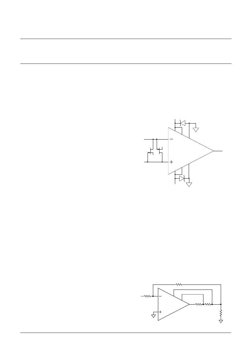
OVERVOLTAGE PROTECTION
Although the MP230 can withstand differential input voltages
up to ±25V, in some applications additional external protection
may be needed. 1N4148 signal diodes connected anti-parallel
across the input pins is usually sufficient. In more demanding
applications where bias current is important diode connected
JFETs such as 2N4416 will be required. See Q1 and Q2 in
Figure 1. In either case the differential input voltage will be
clamped to ±0.7V. This is sufficient overdrive to produce the
maximum power bandwidth. Some applications will also need
over-voltage protection devices connected to the power supply
rails. Unidirectional zener diode transient suppressors are
recommended. The zeners clamp transients to voltages within
the power supply rating and also clamp power supply reversals
to ground. Whether the zeners are used or not the system
power supply should be evaluated for transient performance
including power-on overshoot and power-off polarity reversals
as well as line regulation. See Z1 and Z2 in Figure 1.
POWER SUPPLY BYPASSING
Bypass capacitors to power supply terminals +V
S
and -V
S
must be connected physically close to the pins to prevent local
parasitic oscillation in the output stage of the MP230. Use
electrolytic capacitors at least 10μF per output amp required.
Bypass the electrolytic capacitors with high quality ceramic
capacitors 0.1μF or greater. In most applications power
supply terminals +V
B
and -V
B
will be connected to +V
S
and -V
S
respectively. Although +V
and -V
are bypassed internally it
is recommended to bypass +V
B
and -V
B
with 0.1μF externally.
Additionally, ground pins 2 and 40 must be connected to the
system signal ground.
CURRENT LIMIT
The two current limit sense lines are to be connected directly
across the current limit sense resistor. For the current limit to
work correctly pin 36 must be connected to the amplifier output
side and pin 35 connected to the load side of the current limit
resistor R
LIM
as shown in Figure 2. This connection will bypass
相关PDF资料 |
PDF描述 |
|---|---|
| MP240 | POWER OPERATIONAL AMPLIFIER |
| MP3-306 | Ultra-Fast-Recovery Rectifier Diodes |
| MP38 | POWER OPERATIONAL AMPLIFIER |
| MP38A | POWER OPERATIONAL AMPLIFIER |
| MP39 | POWER OPERATIONAL AMPLIFIER |
相关代理商/技术参数 |
参数描述 |
|---|---|
| MP2303 | 制造商:MPS 制造商全称:Monolithic Power Systems 功能描述:3A, 28V, 340KHz Synchronous Rectified Step-Down Converter |
| MP2303_06 | 制造商:MPS 制造商全称:Monolithic Power Systems 功能描述:3A, 28V, 340KHz Synchronous Rectified Step-Down Converter |
| MP2303ADN-LF | 功能描述:开关变换器、稳压器与控制器 3A, 28V, 360kHz Synchronous Buck RoHS:否 制造商:Texas Instruments 输出电压:1.2 V to 10 V 输出电流:300 mA 输出功率: 输入电压:3 V to 17 V 开关频率:1 MHz 工作温度范围: 安装风格:SMD/SMT 封装 / 箱体:WSON-8 封装:Reel |
| MP2303ADN-LF-Z | 功能描述:开关变换器、稳压器与控制器 3A, 28V, 360kHz Synchronous Buck RoHS:否 制造商:Texas Instruments 输出电压:1.2 V to 10 V 输出电流:300 mA 输出功率: 输入电压:3 V to 17 V 开关频率:1 MHz 工作温度范围: 安装风格:SMD/SMT 封装 / 箱体:WSON-8 封装:Reel |
| MP2303DN | 制造商:MPS 制造商全称:Monolithic Power Systems 功能描述:3A, 28V, 340KHz Synchronous Rectified Step-Down Converter |
发布紧急采购,3分钟左右您将得到回复。