- 您现在的位置:买卖IC网 > PDF目录10930 > MPC5553MZP132 (Freescale Semiconductor)IC MCU MPC5553 REV A 416-PBGA PDF资料下载
参数资料
| 型号: | MPC5553MZP132 |
| 厂商: | Freescale Semiconductor |
| 文件页数: | 6/68页 |
| 文件大小: | 0K |
| 描述: | IC MCU MPC5553 REV A 416-PBGA |
| 产品培训模块: | MPC55xx PitchPak Family |
| 标准包装: | 200 |
| 系列: | MPC55xx Qorivva |
| 核心处理器: | e200z6 |
| 芯体尺寸: | 32-位 |
| 速度: | 132MHz |
| 连通性: | CAN,EBI/EMI,以太网,SCI,SPI |
| 外围设备: | DMA,POR,PWM,WDT |
| 输入/输出数: | 220 |
| 程序存储器容量: | 1.5MB(1.5M x 8) |
| 程序存储器类型: | 闪存 |
| RAM 容量: | 64K x 8 |
| 电压 - 电源 (Vcc/Vdd): | 1.35 V ~ 1.65 V |
| 数据转换器: | A/D 40x12b |
| 振荡器型: | 外部 |
| 工作温度: | -40°C ~ 125°C |
| 封装/外壳: | 416-BBGA |
| 包装: | 托盘 |
| 配用: | MPC5553EVBISYS-ND - KIT EVAL ISYSTEMS MPC5553 MPC5553EVBGHS-ND - KIT EVAL GREEN HILLS SOFTWARE MPC5553EVB-ND - KIT EVAL MPC5553MZP132 MPC5553EVBE-ND - BOARD EVAL FOR MPC5553 |
第1页第2页第3页第4页第5页当前第6页第7页第8页第9页第10页第11页第12页第13页第14页第15页第16页第17页第18页第19页第20页第21页第22页第23页第24页第25页第26页第27页第28页第29页第30页第31页第32页第33页第34页第35页第36页第37页第38页第39页第40页第41页第42页第43页第44页第45页第46页第47页第48页第49页第50页第51页第52页第53页第54页第55页第56页第57页第58页第59页第60页第61页第62页第63页第64页第65页第66页第67页第68页
MPC5553 Microcontroller Data Sheet, Rev. 4
Electrical Characteristics
Freescale Semiconductor
14
3.7.1
Input Value of Pins During POR Dependent on VDD33
When powering up the device, VDD33 must not lag the latest VDDSYN or RESET power pin (VDDEH6) by
more than the VDD33 lag specification listed in Table 6, spec 8. This avoids accidentally selecting the
bypass clock mode because the internal versions of PLLCFG[0:1] and RSTCFG are not powered and
therefore cannot read the default state when POR negates. VDD33 can lag VDDSYN or the RESET power
pin (VDDEH6), but cannot lag both by more than the VDD33 lag specification. This VDD33 lag specification
applies during power up only. VDD33 has no lead or lag requirements when powering down.
3.7.2
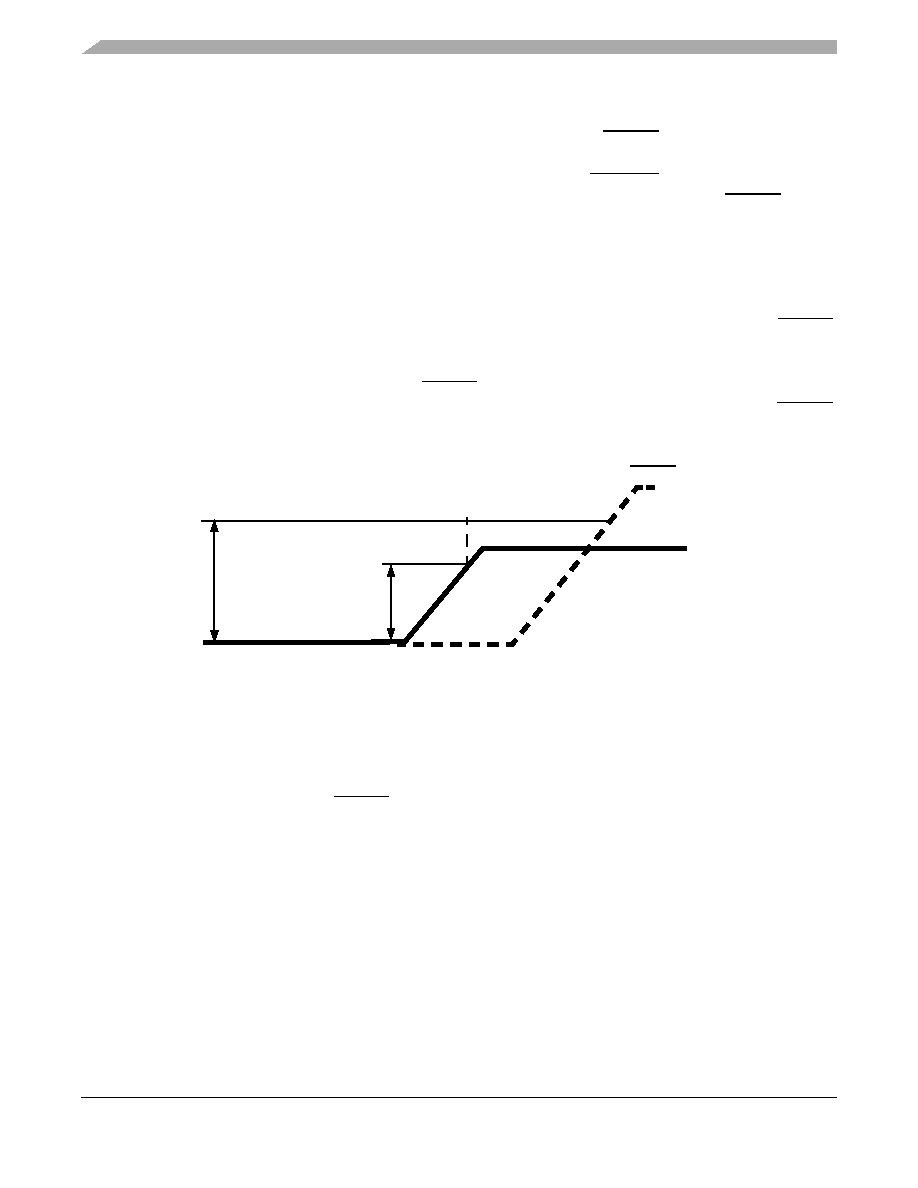
Power-Up Sequence (VRC33 Grounded)
The 1.5 V VDD power supply must rise to 1.35 V before the 3.3 V VDDSYN power supply and the RESET
power supply rises above 2.0 V. This ensures that digital logic in the PLL for the 1.5 V power supply does
not begin to operate below the specified operation range lower limit of 1.35 V. Because the internal 1.5 V
POR is disabled, the internal 3.3 V POR or the RESET power POR must hold the device in reset. Since
they can negate as low as 2.0 V, VDD must be within specification before the 3.3 V POR and the RESET
POR negate.
Figure 3. Power-Up Sequence (VRC33 Grounded)
3.7.3
Power-Down Sequence (VRC33 Grounded)
The only requirement for the power-down sequence with VRC33 grounded is if VDD decreases to less than
its operating range, VDDSYN or the RESET power must decrease to less than 2.0 V before the VDD power
increases to its operating range. This ensures that the digital 1.5 V logic, which is reset only by an ORed
POR and can cause the 1.5 V supply to decrease less than its specification value, resets correctly. See
Table 6, footnote 1.
VDDSYN and RESET Power
VDD
2.0 V
1.35 V
VDD must reach 1.35 V before VDDSYN and the RESET power reach 2.0 V
相关PDF资料 |
PDF描述 |
|---|---|
| MC9328MX1CVM15 | IC MCU I.MX 150MHZ 256-MAPBGA |
| MC68331CEH16 | IC MCU 32BIT 16MHZ 132-PQFP |
| VE-223-IX-F1 | CONVERTER MOD DC/DC 24V 75W |
| VE-222-IX-F4 | CONVERTER MOD DC/DC 15V 75W |
| VE-222-IX-F3 | CONVERTER MOD DC/DC 15V 75W |
相关代理商/技术参数 |
参数描述 |
|---|---|
| MPC5553MZP132R2 | 制造商:FREESCALE 制造商全称:Freescale Semiconductor, Inc 功能描述:Microcontroller |
| MPC5553MZP80 | 制造商:Freescale Semiconductor 功能描述:MPC5553 416 - SNPB - Trays |
| MPC5553MZP80R2 | 制造商:FREESCALE 制造商全称:Freescale Semiconductor, Inc 功能描述:Microcontroller |
| MPC5553MZQ112 | 制造商:FREESCALE 制造商全称:Freescale Semiconductor, Inc 功能描述:Microcontroller |
| MPC5553MZQ112R2 | 制造商:FREESCALE 制造商全称:Freescale Semiconductor, Inc 功能描述:Microcontroller |
发布紧急采购,3分钟左右您将得到回复。