- 您现在的位置:买卖IC网 > PDF目录80568 > MPC5646CCF0VLU8 (FREESCALE SEMICONDUCTOR INC) 32-BIT, FLASH, 80 MHz, MICROCONTROLLER, PQFP176 PDF资料下载
参数资料
| 型号: | MPC5646CCF0VLU8 |
| 厂商: | FREESCALE SEMICONDUCTOR INC |
| 元件分类: | 微控制器/微处理器 |
| 英文描述: | 32-BIT, FLASH, 80 MHz, MICROCONTROLLER, PQFP176 |
| 封装: | 24 X 24 MM, 1.40 MM HEIGHT, 0.50 MM PITCH, ROHS COMPLIANT, LQFP-176 |
| 文件页数: | 13/115页 |
| 文件大小: | 783K |
| 代理商: | MPC5646CCF0VLU8 |
第1页第2页第3页第4页第5页第6页第7页第8页第9页第10页第11页第12页当前第13页第14页第15页第16页第17页第18页第19页第20页第21页第22页第23页第24页第25页第26页第27页第28页第29页第30页第31页第32页第33页第34页第35页第36页第37页第38页第39页第40页第41页第42页第43页第44页第45页第46页第47页第48页第49页第50页第51页第52页第53页第54页第55页第56页第57页第58页第59页第60页第61页第62页第63页第64页第65页第66页第67页第68页第69页第70页第71页第72页第73页第74页第75页第76页第77页第78页第79页第80页第81页第82页第83页第84页第85页第86页第87页第88页第89页第90页第91页第92页第93页第94页第95页第96页第97页第98页第99页第100页第101页第102页第103页第104页第105页第106页第107页第108页第109页第110页第111页第112页第113页第114页第115页
Package pinouts and signal descriptions
MPC5646C Microcontroller Datasheet, Rev. 4
Preliminary—Subject to Change Without Notice
Freescale Semiconductor
11
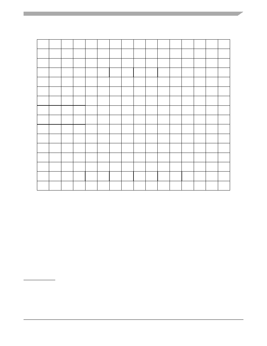
Figure 4. 256-pin BGA configuration
3.1
Pad types
In the device the following types of pads are available for system pins and functional port pins:
S = Slow1
M = Medium1, 2
1234
5678
9
10
11
12
13
14
15
16
A
PC[15]
PB[2]
PC[13]
PI[1]
PE[7]
PH[8]
PE[2]
PE[4]
PC[4]
PE[3]
PH[9]
PI[4]
PH[11]
PE[14]
PA[10]
PG[11]
A
B
PH[13]
PC[14]
PC[8]
PC[12]
PI[3]
PE[6]
PH[5]
PE[5]
PC[5]
PC[0]
PC[2]
PH[12]
PG[10]
PA[11]
PA[9]
PA[8]
B
C
PH[14]
VDD_HV_
A
PC[9]
PL[0]
PI[0]
PH[7]
PH[6]
VSS_LV
VDD_HV_
A
PA[5]
PC[3]
PE[15]
PG[14]
PE[12]
PA[7]
PE[13]
C
D
PG[5]
PI[6]
PJ[4]
PB[3]
PK[15]
PI[2]
PH[4]
VDD_LV
PC[1]
PH[10]
PA[6]
PI[5]
PG[15]
PF[14]
PF[15]
PH[2]
D
E
PG[3]
PI[7]
PH[15]
PG[2]
VDD_LV
VSS_LV
PK[10]
PK[9]
PM[1]
PM[0]
PL[15]
PL[14]
PG[0]
PG[1]
PH[0]
VDD_HV_
A
E
F
PA[2]
PG[4]
PA[1]
PE[1]
PL[2]
PM[6]
PL[1]
PK[11]
PM[5]
PL[13]
PL[12]
PM[2]
PH[1]
PH[3]
PG[12]
PG[13]
F
G
PE[8]
PE[0]
PE[10]
PA[0]
PL[3]
VSS_HV
PK[12]
VDD_HV_
B
PI[13]
PI[12]
PA[3]
G
H
PE[9]
VDD_HV_
A
PE[11]
PK[1]
PL[4]
VSS_LV
VSS_HV
PK[13]
VDD_HV_
A
VDD_LV
VSS_LV
PI[11]
H
J
VSS_HV
VRC_CTR
L
VDD_LV
PG[9]
PL[5]
VSS_LV
VSS_HV
PK[14]
PD[15]
PI[8]
PI[9]
PI[10]
J
K
RESET
VSS_LV
PG[8]
PC[11]
PL[6]
VSS_LV
VDD_LV
PM[3]
PD[14]
PD[13]
PB[14]
PB[15]
K
L
PC[10]
PG[7]
PB[0]
PK[2]
PL[7]
VSS_LV
VDD_LV
PM[4]
PD[12]
PB[12]
PB[13]
VDD_HV_
ADC1
L
M
PG[6]
PB[1]
PK[4]
PF[9]
PK[5]
PK[6]
PK[7]
PK[8]
PL[8]
PL[9]
PL[10]
PL[11]
PB[11]
PD[10]
PD[11]
VSS_HV_
ADC1
M
N
PK[3]
PF[8]
PC[6]
PC[7]
PJ[13]
VDD_HV_
A
PB[10]
PF[6]
VDD_HV_
A
PJ[1]
PD[2]
PJ[5]
PB[5]
PB[6]
PJ[6]
PD[9]
N
P
PF[12]
PF[10]
PF[13]
PA[14]
PJ[9]
PA[12]
PF[0]
PF[5]
PF[7]
PJ[3]
PI[15]
PD[4]
PD[7]
PD[8]
PJ[8]
PJ[7]
P
R
PF[11]
PA[15]
PJ[11]
PJ[15]
PA[13]
PF[2]
PF[3]
PF[4]
VDD_LV
PJ[2]
PJ[0]
PD[0]
PD[3]
PD[6]
VDD_HV_
ADC0
PB[7]
R
T
PJ[12]
PA[4]
PK[0]
PJ[14]
PJ[10]
PF[1]
XTAL
EXTAL
VSS_LV
PB[9]
PB[8]
PI[14]
PD[1]
PD[5]
VSS_HV_
ADC0
PB[4]
T
1234
5678
9
10
11
12
13
14
15
16
Notes:
1) VDD_HV_B supplies the IO voltage domain for the pins PE[12], PA[11], PA[10], PA[9], PA[8], PA[7], PE[13], PF[14], PF[15], PG[0],
PG[1], PH[3], PH[2], PH[1], PH[0], PG[12], PG[13], and PA[3].
2)Availability of port pin alternate functions depends on product selection.
1. See the I/O pad electrical characteristics in the device data sheet for details.
2. All medium and fast pads are in slow configuration by default at reset and can be configured as fast or medium. For example,
Fast/Medium pad will be Medium by default at reset. Similarly, Slow/Medium pad will be Slow by default. Only exception is PC[1]
which is in medium configuration by default (refer to PCR.SRC in the reference manual, Pad Configuration Registers
(PCR0—PCR198)).
相关PDF资料 |
PDF描述 |
|---|---|
| MPC5646CF0VLU8 | 32-BIT, FLASH, 80 MHz, MICROCONTROLLER, PQFP176 |
| MPC5604CF1MLQ4 | MICROCONTROLLER, PQFP144 |
| MPC5602PEF0VLH4 | 32-BIT, FLASH, 64 MHz, RISC MICROCONTROLLER, PQFP64 |
| MPC8272VRM | 32-BIT, EPROM, 266 MHz, RISC MICROCONTROLLER, PBGA516 |
| MPC8272ZQM | 32-BIT, EPROM, 266 MHz, RISC MICROCONTROLLER, PBGA516 |
相关代理商/技术参数 |
参数描述 |
|---|---|
| MPC564AADPT176 | 功能描述:开发板和工具包 - 其他处理器 ANDORRA ADAPT RoHS:否 制造商:Freescale Semiconductor 产品:Development Systems 工具用于评估:P3041 核心:e500mc 接口类型:I2C, SPI, USB 工作电源电压: |
| MPC564AADPT208 | 制造商:Freescale Semiconductor 功能描述:ANDORRA ADAPSOLDERED |
| MPC564AKIT176 | 功能描述:开发板和工具包 - 其他处理器 ANDORRA 176QFP KIT RoHS:否 制造商:Freescale Semiconductor 产品:Development Systems 工具用于评估:P3041 核心:e500mc 接口类型:I2C, SPI, USB 工作电源电压: |
| MPC564AKIT176S | 制造商:Freescale Semiconductor 功能描述:MPC564XA 176 LQFP SOCKET EVAL KIT 制造商:Freescale Semiconductor 功能描述:MPC564XA, 176 LQFP SOCKET, EVAL KIT |
| MPC564AKIT208 | 制造商:Freescale Semiconductor 功能描述:ANDORRA 208BGA KIT |
发布紧急采购,3分钟左右您将得到回复。