- 您现在的位置:买卖IC网 > PDF目录4069 > MPC8313CVRAGDB (Freescale Semiconductor)MPU POWERQUICC II PRO 516-PBGA PDF资料下载
参数资料
| 型号: | MPC8313CVRAGDB |
| 厂商: | Freescale Semiconductor |
| 文件页数: | 91/99页 |
| 文件大小: | 0K |
| 描述: | MPU POWERQUICC II PRO 516-PBGA |
| 标准包装: | 40 |
| 系列: | MPC83xx |
| 处理器类型: | 32-位 MPC83xx PowerQUICC II Pro |
| 速度: | 400MHz |
| 电压: | 0.95 V ~ 1.05 V |
| 安装类型: | 表面贴装 |
| 封装/外壳: | 516-BBGA 裸露焊盘 |
| 供应商设备封装: | 516-PBGAPGE(27x27) |
| 包装: | 托盘 |
第1页第2页第3页第4页第5页第6页第7页第8页第9页第10页第11页第12页第13页第14页第15页第16页第17页第18页第19页第20页第21页第22页第23页第24页第25页第26页第27页第28页第29页第30页第31页第32页第33页第34页第35页第36页第37页第38页第39页第40页第41页第42页第43页第44页第45页第46页第47页第48页第49页第50页第51页第52页第53页第54页第55页第56页第57页第58页第59页第60页第61页第62页第63页第64页第65页第66页第67页第68页第69页第70页第71页第72页第73页第74页第75页第76页第77页第78页第79页第80页第81页第82页第83页第84页第85页第86页第87页第88页第89页第90页当前第91页第92页第93页第94页第95页第96页第97页第98页第99页
MPC8313E PowerQUICC II Pro Processor Hardware Specifications, Rev. 4
Freescale Semiconductor
91
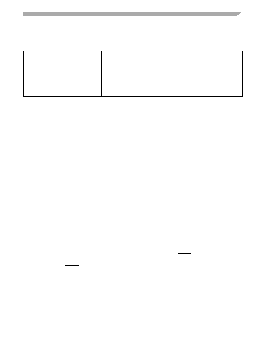
This table summarizes the signal impedance targets. The driver impedance are targeted at minimum VDD,
nominal NVDD, 105C.
22.7
Configuration Pin Muxing
The MPC8313E provides the user with power-on configuration options which can be set through the use
of external pull-up or pull-down resistors of 4.7 k
on certain output pins (see customer visible
configuration pins). These pins are generally used as output only pins in normal operation.
While HRESET is asserted however, these pins are treated as inputs. The value presented on these pins
while HRESET is asserted, is latched when PORESET deasserts, at which time the input receiver is
disabled and the I/O circuit takes on its normal function. Careful board layout with stubless connections
to these pull-up/pull-down resistors coupled with the large value of the pull-up/pull-down resistor should
minimize the disruption of signal quality or speed for output pins thus configured.
22.8
Pull-Up Resistor Requirements
The MPC8313E requires high resistance pull-up resistors (10 k
is recommended) on open drain type pins
including I2C, and IPIC (integrated programmable interrupt controller).
Correct operation of the JTAG interface requires configuration of a group of system control pins as
demonstrated in Figure 61. Care must be taken to ensure that these pins are maintained at a valid deasserted
state under normal operating conditions because most have asynchronous behavior and spurious assertion,
which give unpredictable results.
Refer to the PCI 2.2 Specification, for all pull-ups required for PCI.
22.9
JTAG Configuration Signals
Boundary scan testing is enabled through the JTAG interface signals. The TRST signal is optional in
IEEE 1149.1, but is provided on any Freescale devices that are built on Power Architecture technology.
The device requires TRST to be asserted during reset conditions to ensure the JTAG boundary logic does
not interfere with normal chip operation. While it is possible to force the TAP controller to the reset state
using only the TCK and TMS signals, systems generally assert TRST during power-on reset. Because the
JTAG interface is also used for accessing the common on-chip processor (COP) function, simply tying
TRST to PORESET is not practical.
Table 71. Impedance Characteristics
Impedance
Local Bus, Ethernet,
DUART, Control,
Configuration, Power
Management
PCI Signals
(Not Including PCI
Output Clocks)
PCI Output Clocks
(Including
PCI_SYNC_OUT)
DDR DRAM
Symbol
Unit
RN
42 Target
25 Target
42 Target
20 Target
Z0
RP
42 Target
25 Target
42 Target
20 Target
Z0
Differential
NA
ZDIFF
相关PDF资料 |
PDF描述 |
|---|---|
| FSM43DSEI-S13 | CONN EDGECARD 86POS .156 EXTEND |
| FI-X20M-NPB | CONN PLUG FFC 1MM 20POS |
| HMC65DRAN-S734 | CONN EDGECARD 130PS .100 R/A PCB |
| HMC65DRAH-S734 | CONN EDGECARD 130PS .100 R/A PCB |
| ABB92DHBS-S329 | CONN EDGECARD 184POS R/A .050 SL |
相关代理商/技术参数 |
参数描述 |
|---|---|
| MPC8313CVRAGDC | 功能描述:微处理器 - MPU 8313 REV2.2 NO ENC EXT RoHS:否 制造商:Atmel 处理器系列:SAMA5D31 核心:ARM Cortex A5 数据总线宽度:32 bit 最大时钟频率:536 MHz 程序存储器大小:32 KB 数据 RAM 大小:128 KB 接口类型:CAN, Ethernet, LIN, SPI,TWI, UART, USB 工作电源电压:1.8 V to 3.3 V 最大工作温度:+ 85 C 安装风格:SMD/SMT 封装 / 箱体:FBGA-324 |
| MPC8313CVRGDD | 制造商:FREESCALE 制造商全称:Freescale Semiconductor, Inc 功能描述:PowerQUICC? II Pro Processor Hardware Specifications |
| MPC8313CVRGDDA | 制造商:FREESCALE 制造商全称:Freescale Semiconductor, Inc 功能描述:PowerQUICC? II Pro Processor Hardware Specifications |
| MPC8313CVRGDDB | 制造商:FREESCALE 制造商全称:Freescale Semiconductor, Inc 功能描述:PowerQUICC? II Pro Processor Hardware Specifications |
| MPC8313CVRGDF | 制造商:FREESCALE 制造商全称:Freescale Semiconductor, Inc 功能描述:PowerQUICC? II Pro Processor Hardware Specifications |
发布紧急采购,3分钟左右您将得到回复。