- 您现在的位置:买卖IC网 > PDF目录4076 > MPC8315CVRADDA (Freescale Semiconductor)MPU POWERQUICC II PRO 620-PBGA PDF资料下载
参数资料
| 型号: | MPC8315CVRADDA |
| 厂商: | Freescale Semiconductor |
| 文件页数: | 15/106页 |
| 文件大小: | 0K |
| 描述: | MPU POWERQUICC II PRO 620-PBGA |
| 标准包装: | 36 |
| 系列: | MPC83xx |
| 处理器类型: | 32-位 MPC83xx PowerQUICC II Pro |
| 速度: | 266MHz |
| 电压: | 1V |
| 安装类型: | 表面贴装 |
| 封装/外壳: | 620-BBGA 裸露焊盘 |
| 供应商设备封装: | 620-PBGA(29x29) |
| 包装: | 托盘 |
第1页第2页第3页第4页第5页第6页第7页第8页第9页第10页第11页第12页第13页第14页当前第15页第16页第17页第18页第19页第20页第21页第22页第23页第24页第25页第26页第27页第28页第29页第30页第31页第32页第33页第34页第35页第36页第37页第38页第39页第40页第41页第42页第43页第44页第45页第46页第47页第48页第49页第50页第51页第52页第53页第54页第55页第56页第57页第58页第59页第60页第61页第62页第63页第64页第65页第66页第67页第68页第69页第70页第71页第72页第73页第74页第75页第76页第77页第78页第79页第80页第81页第82页第83页第84页第85页第86页第87页第88页第89页第90页第91页第92页第93页第94页第95页第96页第97页第98页第99页第100页第101页第102页第103页第104页第105页第106页
MPC8315E PowerQUICC II Pro Processor Hardware Specifications, Rev. 2
16
Freescale Semiconductor
Clock Input Timing
5.1
DC Electrical Characteristics
This table provides the clock input (SYS_CLK_IN/PCI_SYNC_IN) DC timing specifications for the
MPC8315E.
5.2
AC Electrical Characteristics
The primary clock source for the MPC8315E can be one of two inputs, SYS_CLK_IN or PCI_CLK,
depending on whether the device is configured in PCI host or PCI agent mode. This table provides the
clock input (SYS_CLK_IN/PCI_CLK) AC timing specifications for the MPC8315E.
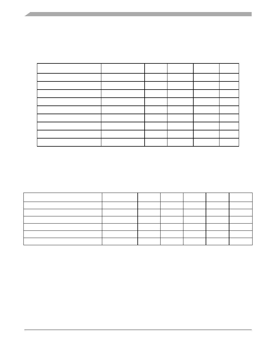
Table 6. SYS_CLK_IN DC Electrical Characteristics
Parameter
Condition
Symbol
Min
Max
Unit
Input high voltage
—
VIH
2.4
NVDD + 0.3
V
Input low voltage
—
VIL
-0.3
0.4
V
SYS_CLK_IN input current
0 V
V
IN NVDD
IIN
—±10
A
SYS_XTAL_IN input current
0 V
V
IN NVDD
IIN
—±40
A
PCI_SYNC_IN input current
0 V
V
IN NVDD
IIN
—±10
A
RTC_CLK input current
0 V
V
IN NVDD
IIN
—±10
A
USB_CLK_IN input current
0 V
V
IN NVDD
IIN
—±10
A
USB_XTAL_IN input current
0 V
V
IN NVDD
IIN
—±40
A
SATA_CLK_IN input current
0 V
V
IN NVDD
IIN
—±10
A
Table 7. SYS_CLK_IN AC Timing Specifications
Parameter/Condition
Symbol
Min
Typical
Max
Unit
Note
SYS_CLK_IN/PCI_CLK frequency
fSYS_CLK_IN
24
—
66.67
MHz
1, 6, 7
SYS_CLK_IN/PCI_CLK cycle time
tSYS_CLK_IN
15
—
41.6
ns
6
SYS_CLK_IN rise and fall time
tKH, tKL
0.6
—
4
ns
2, 6
PCI_CLK rise and fall time
tPCH, tPCL
0.6
0.8
1.2
ns
2
SYS_CLK_IN/PCI_CLK duty cycle
tKHK/tSYS_CLK_IN
40
—
60
%
3, 6
SYS_CLK_IN/PCI_CLK jitter
—
±150
ps
4, 5, 6
Note:
1. Caution: The system, core, and security block must not exceed their respective maximum or minimum operating
frequencies.
2. Rise and fall times for SYS_CLK_IN/PCI_CLK are specified at 20% to 80% of signal swing.
3. Timing is guaranteed by design and characterization.
4. This represents the total input jitter—short term and long term—and is guaranteed by design.
5. The SYS_CLK_IN/PCI_CLK driver’s closed loop jitter bandwidth should be <500 kHz at –20 dB. The bandwidth must be set
low to allow cascade-connected PLL-based devices to track SYS_CLK_IN drivers with the specified jitter.
6. The parameter names PCI_CLK and PCI_SYNC_IN are used interchangeably in this document.
7. Spread spectrum is allowed up to 1% down-spread at 33kHz.(max. rate).
相关PDF资料 |
PDF描述 |
|---|---|
| IDT7005S17J8 | IC SRAM 64KBIT 17NS 68PLCC |
| MPC859DSLCZP66A | IC MPU POWERQUICC 66MHZ 357PBGA |
| MPC8323CVRADDC | IC MPU PWRQUICC II 516-PBGA |
| MPC8323ZQAFDC | IC MPU PWRQUICC II 516-PBGA |
| MPC8323VRAFDC | IC MPU PWRQUICC II 516-PBGA |
相关代理商/技术参数 |
参数描述 |
|---|---|
| MPC8315CVRAFDA | 功能描述:微处理器 - MPU NON-ENCRYPT RoHS:否 制造商:Atmel 处理器系列:SAMA5D31 核心:ARM Cortex A5 数据总线宽度:32 bit 最大时钟频率:536 MHz 程序存储器大小:32 KB 数据 RAM 大小:128 KB 接口类型:CAN, Ethernet, LIN, SPI,TWI, UART, USB 工作电源电压:1.8 V to 3.3 V 最大工作温度:+ 85 C 安装风格:SMD/SMT 封装 / 箱体:FBGA-324 |
| MPC8315CVRAGDA | 功能描述:微处理器 - MPU NON-ENCRYPT RoHS:否 制造商:Atmel 处理器系列:SAMA5D31 核心:ARM Cortex A5 数据总线宽度:32 bit 最大时钟频率:536 MHz 程序存储器大小:32 KB 数据 RAM 大小:128 KB 接口类型:CAN, Ethernet, LIN, SPI,TWI, UART, USB 工作电源电压:1.8 V to 3.3 V 最大工作温度:+ 85 C 安装风格:SMD/SMT 封装 / 箱体:FBGA-324 |
| MPC8315E | 制造商:FREESCALE 制造商全称:Freescale Semiconductor, Inc 功能描述:PowerQUICC? II Pro Processor Hardware Specifications |
| MPC8315ECVRADDA | 功能描述:微处理器 - MPU ENCRYPT RoHS:否 制造商:Atmel 处理器系列:SAMA5D31 核心:ARM Cortex A5 数据总线宽度:32 bit 最大时钟频率:536 MHz 程序存储器大小:32 KB 数据 RAM 大小:128 KB 接口类型:CAN, Ethernet, LIN, SPI,TWI, UART, USB 工作电源电压:1.8 V to 3.3 V 最大工作温度:+ 85 C 安装风格:SMD/SMT 封装 / 箱体:FBGA-324 |
| MPC8315ECVRAFDA | 功能描述:微处理器 - MPU ENCRYPT RoHS:否 制造商:Atmel 处理器系列:SAMA5D31 核心:ARM Cortex A5 数据总线宽度:32 bit 最大时钟频率:536 MHz 程序存储器大小:32 KB 数据 RAM 大小:128 KB 接口类型:CAN, Ethernet, LIN, SPI,TWI, UART, USB 工作电源电压:1.8 V to 3.3 V 最大工作温度:+ 85 C 安装风格:SMD/SMT 封装 / 箱体:FBGA-324 |
发布紧急采购,3分钟左右您将得到回复。