- 您现在的位置:买卖IC网 > PDF目录4067 > MPC8358CZQAGDGA (Freescale Semiconductor)MPU POWERQUICC II PRO 668-PBGA PDF资料下载
参数资料
| 型号: | MPC8358CZQAGDGA |
| 厂商: | Freescale Semiconductor |
| 文件页数: | 70/95页 |
| 文件大小: | 0K |
| 描述: | MPU POWERQUICC II PRO 668-PBGA |
| 标准包装: | 36 |
| 系列: | MPC83xx |
| 处理器类型: | 32-位 MPC83xx PowerQUICC II Pro |
| 速度: | 400MHz |
| 电压: | 1.2V |
| 安装类型: | 表面贴装 |
| 封装/外壳: | 668-BBGA 裸露焊盘 |
| 供应商设备封装: | 668-PBGA-PGE(29x29) |
| 包装: | 托盘 |
第1页第2页第3页第4页第5页第6页第7页第8页第9页第10页第11页第12页第13页第14页第15页第16页第17页第18页第19页第20页第21页第22页第23页第24页第25页第26页第27页第28页第29页第30页第31页第32页第33页第34页第35页第36页第37页第38页第39页第40页第41页第42页第43页第44页第45页第46页第47页第48页第49页第50页第51页第52页第53页第54页第55页第56页第57页第58页第59页第60页第61页第62页第63页第64页第65页第66页第67页第68页第69页当前第70页第71页第72页第73页第74页第75页第76页第77页第78页第79页第80页第81页第82页第83页第84页第85页第86页第87页第88页第89页第90页第91页第92页第93页第94页第95页
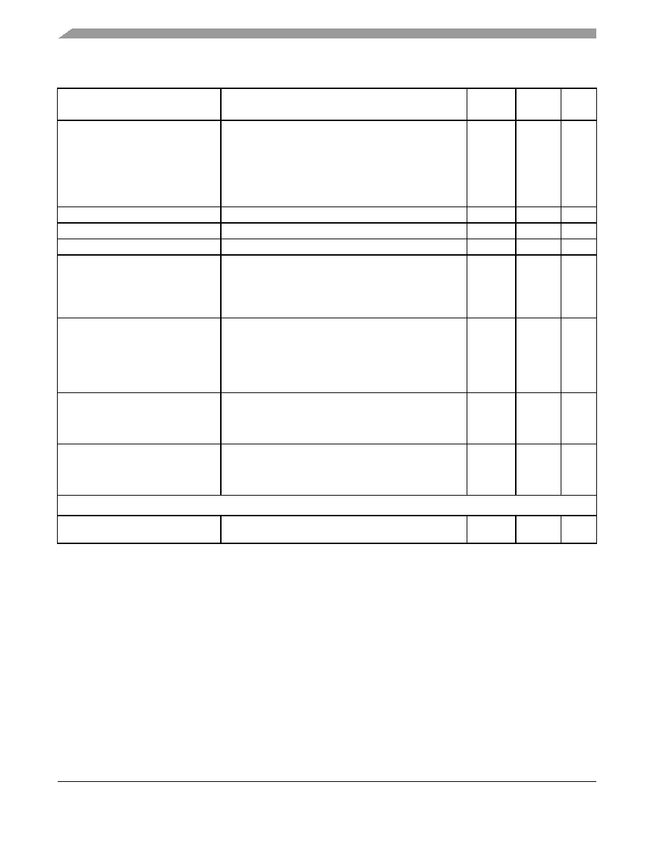
MPC8358E PowerQUICC II Pro Processor Revision 2.1 PBGA Silicon Hardware Specifications, Rev. 3
72
Freescale Semiconductor
Package and Pin Listings
GVDD
C19, C22, C25, G24, J18, J19, J20, J24, K19, K20, K26,
L20, M20, M26, N19, N20, P20, P27, R20, T19, T20, T27,
U19, U20, U25, V19, V20, W20, W26, Y20, AA24, AB28,
AC21, AC28, AD28, AF21, AF25
Power for
DDR
DRAM
I/O
Voltage
(2.5 V or
1.8 V)
GVDD
—
LVDD0F3, J9
—
LVDD0—
LVDD1P3, P10
—
LVDD110
LVDD2R4, R10
—
LVDD210
VDD
M12, M13, M16, M17, N10, N12, N13, N14, N15, N16,
N17, P12, P13, P14, P15, P16, P17, R12, R13, R16,
R17, T12, T13, T16, T17, U12, U13, U14, U15, U16, U17,
V12, V13, V16, V17, W11, W12, W13, W15, W16, W17,
Y16, Y17
Power for
Core
(1.2 V)
VDD
—
OVDD
C6, C12, D17, J11, J13, J14, K3, K9, K10, K12, K15,
K16, L10, M9, N9, T9, U9, V3, V10, W9, W10, W14, Y9,
Y10, Y12, Y13, Y15, AA3, AE6, AE16, AF11, AF20
PCI,
10/100
Ethernet,
and other
Standard
(3.3 V)
OVDD
—
MVREF1
J27
I
DDR
Referenc
e
Voltage
—
MVREF2
Y24
I
DDR
Referenc
e
Voltage
—
No Connect
NC
F23, G23, H23, J23, K23, L23, M23, N23, P23, R23, T23,
U23, V23, W23, Y23, AA23, AB23, AC23
——
—
Notes:
1. This pin is an open drain signal. A weak pull-up resistor (1 k
Ω) should be placed on this pin to OVDD.
2. This pin is an open drain signal. A weak pull-up resistor (2–10 k
Ω) should be placed on this pin to OVDD.
3. This output is actively driven during reset rather than being three-stated during reset.
4. These JTAG pins have weak internal pull-up P-FETs that are always enabled.
5.This pin should have a weak pull up if the chip is in PCI host mode. Follow PCI specifications recommendation.
6. These are On Die Termination pins, used to control DDR2 memories internal termination resistance.
7. This pin must always be tied to GND.
8. This pin must always be left not connected.
9. This pin must always be tied to GVDD.
10. Refers to
MPC8360E PowerQUICC II Pro Integrated Communications Processor Reference Manual section on “RGMII
Pins” for information about the two UCC2 Ethernet interface options.
11. It is recommended that MDIC0 be tied to GND using an 18.2
Ω resistor and MDIC1 be tied to DDR power using an 18.2 Ω
resistor for DDR2.
Table 65. MPC8358E PBGA Pinout Listing (continued)
Signal
Package Pin Number
Pin Type
Power
Supply
Notes
相关PDF资料 |
PDF描述 |
|---|---|
| MPC8358CVRAGDGA | MPU POWERQUICC II PRO 668-PBGA |
| MPC8377CVRAJFA | MPU POWERQUICC II 533MHZ 689PBGA |
| IDT70V06S55J8 | IC SRAM 128KBIT 55NS 68PLCC |
| IDT7006S55J8 | IC SRAM 128KBIT 55NS 68PLCC |
| MPC8272VRTMFA | IC MPU POWERQUICC II 516-PBGA |
相关代理商/技术参数 |
参数描述 |
|---|---|
| MPC8358CZUADDE | 功能描述:微处理器 - MPU 8360 TBGA NON-ENCRP RoHS:否 制造商:Atmel 处理器系列:SAMA5D31 核心:ARM Cortex A5 数据总线宽度:32 bit 最大时钟频率:536 MHz 程序存储器大小:32 KB 数据 RAM 大小:128 KB 接口类型:CAN, Ethernet, LIN, SPI,TWI, UART, USB 工作电源电压:1.8 V to 3.3 V 最大工作温度:+ 85 C 安装风格:SMD/SMT 封装 / 箱体:FBGA-324 |
| MPC8358CZUADDEA | 功能描述:微处理器 - MPU 8360 TBGA C NON-ENCRP RoHS:否 制造商:Atmel 处理器系列:SAMA5D31 核心:ARM Cortex A5 数据总线宽度:32 bit 最大时钟频率:536 MHz 程序存储器大小:32 KB 数据 RAM 大小:128 KB 接口类型:CAN, Ethernet, LIN, SPI,TWI, UART, USB 工作电源电压:1.8 V to 3.3 V 最大工作温度:+ 85 C 安装风格:SMD/SMT 封装 / 箱体:FBGA-324 |
| MPC8358CZUADDGA | 制造商:FREESCALE 制造商全称:Freescale Semiconductor, Inc 功能描述:MPC8360E/MPC8358E PowerQUICC II Pro Processor |
| MPC8358CZUAGDEA | 制造商:FREESCALE 制造商全称:Freescale Semiconductor, Inc 功能描述:MPC8360E/MPC8358E PowerQUICC II Pro Processor |
| MPC8358CZUAGDG | 功能描述:微处理器 - MPU 8360 TBGA NON-ENCRP RoHS:否 制造商:Atmel 处理器系列:SAMA5D31 核心:ARM Cortex A5 数据总线宽度:32 bit 最大时钟频率:536 MHz 程序存储器大小:32 KB 数据 RAM 大小:128 KB 接口类型:CAN, Ethernet, LIN, SPI,TWI, UART, USB 工作电源电压:1.8 V to 3.3 V 最大工作温度:+ 85 C 安装风格:SMD/SMT 封装 / 箱体:FBGA-324 |
发布紧急采购,3分钟左右您将得到回复。