- 您现在的位置:买卖IC网 > PDF目录17039 > MPC8379E-RDB (Freescale Semiconductor)BOARD REFERENCE FOR MPC837 PDF资料下载
参数资料
| 型号: | MPC8379E-RDB |
| 厂商: | Freescale Semiconductor |
| 文件页数: | 45/117页 |
| 文件大小: | 0K |
| 描述: | BOARD REFERENCE FOR MPC837 |
| 标准包装: | 1 |
| 系列: | PowerQUICC II™ PRO |
| 类型: | MPU |
| 适用于相关产品: | MPC8379 |
| 所含物品: | 板 |
第1页第2页第3页第4页第5页第6页第7页第8页第9页第10页第11页第12页第13页第14页第15页第16页第17页第18页第19页第20页第21页第22页第23页第24页第25页第26页第27页第28页第29页第30页第31页第32页第33页第34页第35页第36页第37页第38页第39页第40页第41页第42页第43页第44页当前第45页第46页第47页第48页第49页第50页第51页第52页第53页第54页第55页第56页第57页第58页第59页第60页第61页第62页第63页第64页第65页第66页第67页第68页第69页第70页第71页第72页第73页第74页第75页第76页第77页第78页第79页第80页第81页第82页第83页第84页第85页第86页第87页第88页第89页第90页第91页第92页第93页第94页第95页第96页第97页第98页第99页第100页第101页第102页第103页第104页第105页第106页第107页第108页第109页第110页第111页第112页第113页第114页第115页第116页第117页
MPC8379E PowerQUICC II Pro Processor Hardware Specifications, Rev. 8
Freescale Semiconductor
33
9.1
USB DC Electrical Characteristics
This table provides the DC electrical characteristics for the ULPI interface at recommended
OVDD = 3.3 V ± 165 mV.
9.2
USB AC Electrical Specifications
This table describes the general timing parameters of the USB interface of the device.
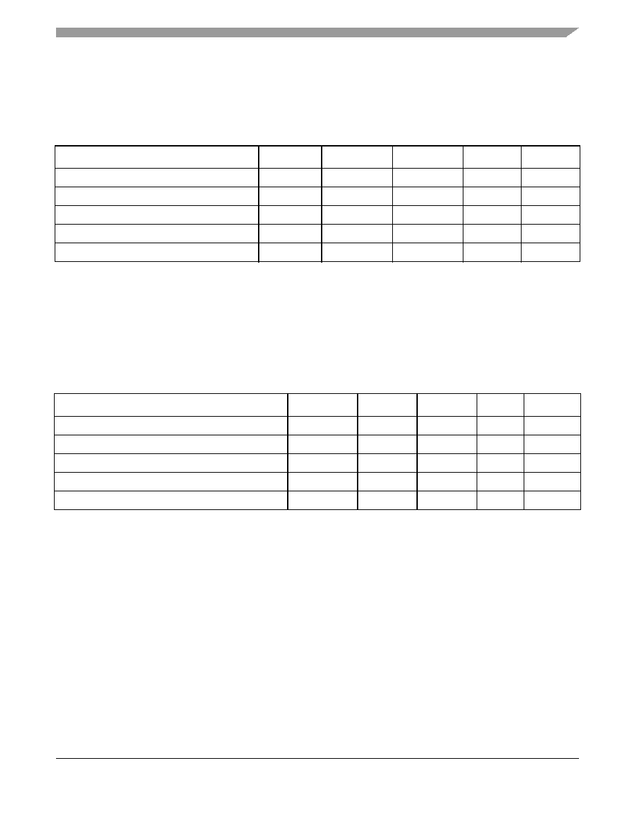
Table 34. USB DC Electrical Characteristics
Parameter
Symbol
Min
Max
Unit
Note
High-level input voltage
VIH
2OVDD + 0.3
V
Low-level input voltage
VIL
–0.3
0.8
V
Input current
IIN
—±30
μA2
High-level output voltage, IOH = –100 μAVOH
OVDD – 0.2
—
V
—
Low-level output voltage, IOL = 100 μAVOL
—0.2
V
—
Notes:
1. The minimum VIL and maximum VIH values are based on the respective minimum and maximum OVIN values found in
Table 35. USB General Timing Parameters (ULPI Mode Only)
Parameter
Symbol 1
Min
Max
Unit
Note
USB clock cycle time
tUSCK
15
—
ns
Input setup to USB clock—all inputs
tUSIVKH
4
—
ns
Input hold to USB clock—all inputs
tUSIXKH
1
—
ns
USB clock to output valid—all outputs
tUSKHOV
—
7
ns
Output hold from USB clock—all outputs
tUSKHOX
2
—
ns
Notes:
1. The symbols for timing specifications follow the pattern of t(First two letters of functional block)(signal)(state) (reference)(state) for inputs
and t(First two letters of functional block)(reference)(state)(signal)(state) for outputs. For example, tUSIXKH symbolizes USB timing (US)
for the input (I) to go invalid (X) with respect to the time the USB clock reference (K) goes high (H). Also, tUSKHOX symbolizes
USB timing (US) for the USB clock reference (K) to go high (H) with respect to the output (O) going invalid (X) or output hold
time.
2. All timings are in reference to the USB clock, USBDR_CLK.
3. All signals are measured from OVDD/2 of the rising edge of the USB clock to 0.4 × OVDD of the signal in question for 3.3-V
signaling levels.
4. Input timings are measured at the pin.
5. For active/float timing measurements, the high impedance or off state is defined to be when the total current delivered
through the component pin is less than or equal to that of the leakage current specification.
相关PDF资料 |
PDF描述 |
|---|---|
| MPC8379E-MDS-PB | BOARD PROCESSOR FOR MDS S |
| MPC8378E-MDS-PB | BOARD PROCESSOR FOR MDS S |
| MPC5553EVBE | BOARD EVAL FOR MPC5553 |
| MPC8323E-MDS-PB | BOARD MODULE DEV SYSTEM 8323 |
| MPC5534EVBE | BOARD EVAL FOR MPC5534 |
相关代理商/技术参数 |
参数描述 |
|---|---|
| MPC8379E-RDBA | 功能描述:开发板和工具包 - 其他处理器 MPC8379E REF DESIGN BD RoHS:否 制造商:Freescale Semiconductor 产品:Development Systems 工具用于评估:P3041 核心:e500mc 接口类型:I2C, SPI, USB 工作电源电压: |
| MPC8379E-RDBA | 制造商:Freescale Semiconductor 功能描述:MPC8379E-RDB Reference Platform |
| MPC8379EVRAFDA | 制造商:FREESCALE 制造商全称:Freescale Semiconductor, Inc 功能描述:PowerQUICC? II Pro Processor Hardware Specifications |
| MPC8379EVRAFFA | 制造商:FREESCALE 制造商全称:Freescale Semiconductor, Inc 功能描述:PowerQUICC? II Pro Processor Hardware Specifications |
| MPC8379EVRAFGA | 制造商:FREESCALE 制造商全称:Freescale Semiconductor, Inc 功能描述:PowerQUICC? II Pro Processor Hardware Specifications |
发布紧急采购,3分钟左右您将得到回复。