- 您现在的位置:买卖IC网 > PDF目录45366 > MPC852TZT80 (FREESCALE SEMICONDUCTOR INC) 32-BIT, 80 MHz, RISC PROCESSOR, PBGA256 PDF资料下载
参数资料
| 型号: | MPC852TZT80 |
| 厂商: | FREESCALE SEMICONDUCTOR INC |
| 元件分类: | 微控制器/微处理器 |
| 英文描述: | 32-BIT, 80 MHz, RISC PROCESSOR, PBGA256 |
| 封装: | PLASTIC, BGA-256 |
| 文件页数: | 13/80页 |
| 文件大小: | 2070K |
| 代理商: | MPC852TZT80 |
第1页第2页第3页第4页第5页第6页第7页第8页第9页第10页第11页第12页当前第13页第14页第15页第16页第17页第18页第19页第20页第21页第22页第23页第24页第25页第26页第27页第28页第29页第30页第31页第32页第33页第34页第35页第36页第37页第38页第39页第40页第41页第42页第43页第44页第45页第46页第47页第48页第49页第50页第51页第52页第53页第54页第55页第56页第57页第58页第59页第60页第61页第62页第63页第64页第65页第66页第67页第68页第69页第70页第71页第72页第73页第74页第75页第76页第77页第78页第79页第80页
MPC852T Hardware Specifications, Rev. 3.1
20
Freescale Semiconductor
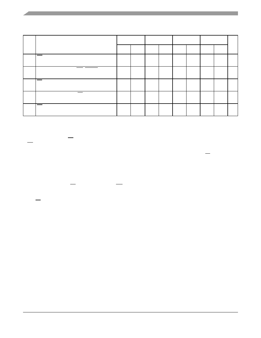
Bus Signal Timing
B39
AS valid to CLKOUT rising edge 10 (MIN = 0.00
x B1 + 7.00)
7.00
—
7.00
—
7.00
—
7.00
—
ns
B40
A(0:31), TSIZ(0:1), RD/WR, BURST, valid to
CLKOUT rising edge (MIN = 0.00 x B1 + 7.00)
7.00
—
7.00
—
7.00
—
7.00
—
ns
B41
TS valid to CLKOUT rising edge (setup time)
(MIN = 0.00 x B1 + 7.00)
7.00
—
7.00
—
7.00
—
7.00
—
ns
B42
CLKOUT rising edge to TS valid (hold time)
(MIN = 0.00 x B1 + 2.00)
2.00
—
2.00
—
2.00
—
2.00
—
ns
B43
AS negation to memory controller signals
negation (MAX = TBD)
—
TBD
—
TBD
—
TBD
—
TBD
ns
1
If the rate of change of the frequency of EXTAL is slow (that is, it does not jump between the minimum and maximum values
in one cycle) or the frequency of the jitter is fast (that is, it does not stay at an extreme value for a long time), then the maximum
allowed jitter on EXTAL can be up to 2%.
2
For part speeds above 50MHz, use 9.80ns for B11a.
3
The timing required for BR input is relevant when the MPC852T is selected to work with internal bus arbiter. The timing for
BG input is relevant when the MPC852T is selected to work with external bus arbiter.
4
For part speeds above 50MHz, use 2ns for B17.
5
The D(0:31) and DP(0:3) input timings B18 and B19 refer to the rising edge of the CLKOUT in which the TA input signal is
asserted.
6
For part speeds above 50MHz, use 2ns for B19.
7
The D(0:31) and DP(0:3) input timings B20 and B21 refer to the falling edge of the CLKOUT. This timing is valid only for read
accesses controlled by chip-selects under control of the UPM in the memory controller, for data beats where DLT3 = 1 in the
UPM RAM words. (This is only the case where data is latched on the falling edge of CLKOUT.)
8
The timing B30 refers to CS when ACS = 00 and to WE(0:3) when CSNT = 0.
9
The signal UPWAIT is considered asynchronous to the CLKOUT and synchronized internally. The timings specified in B37
and B38 are specified to enable the freeze of the UPM output signals as described in Figure 18.
10 The AS signal is considered asynchronous to the CLKOUT. The timing B39 is specified in order to allow the behavior specified
in Figure 21.
Table 9. Bus Operation Timings (continued)
Num
Characteristic
33 MHz
40 MHz
50 MHz
66 MHz
Unit
Min
Max
Min
Max
Min
Max
Min
Max
相关PDF资料 |
PDF描述 |
|---|---|
| MPC852TZT50 | 32-BIT, 50 MHz, RISC PROCESSOR, PBGA256 |
| MPC852TZT80 | 32-BIT, 80 MHz, RISC PROCESSOR, PBGA256 |
| MPC852TVR100 | 32-BIT, 100 MHz, RISC PROCESSOR, PBGA256 |
| MPC8533EVTALJB | 32-BIT, 667 MHz, RISC PROCESSOR, PBGA783 |
| MPC8533VTARFB | 32-BIT, 1067 MHz, RISC PROCESSOR, PBGA783 |
相关代理商/技术参数 |
参数描述 |
|---|---|
| MPC852TZT80A | 功能描述:微处理器 - MPU POWER QUICC II HIP6W RoHS:否 制造商:Atmel 处理器系列:SAMA5D31 核心:ARM Cortex A5 数据总线宽度:32 bit 最大时钟频率:536 MHz 程序存储器大小:32 KB 数据 RAM 大小:128 KB 接口类型:CAN, Ethernet, LIN, SPI,TWI, UART, USB 工作电源电压:1.8 V to 3.3 V 最大工作温度:+ 85 C 安装风格:SMD/SMT 封装 / 箱体:FBGA-324 |
| MPC8533EVTALF | 功能描述:微处理器 - MPU PQ38K 8533E RoHS:否 制造商:Atmel 处理器系列:SAMA5D31 核心:ARM Cortex A5 数据总线宽度:32 bit 最大时钟频率:536 MHz 程序存储器大小:32 KB 数据 RAM 大小:128 KB 接口类型:CAN, Ethernet, LIN, SPI,TWI, UART, USB 工作电源电压:1.8 V to 3.3 V 最大工作温度:+ 85 C 安装风格:SMD/SMT 封装 / 箱体:FBGA-324 |
| MPC8533EVTALFA | 功能描述:微处理器 - MPU PQ38K 8533E RoHS:否 制造商:Atmel 处理器系列:SAMA5D31 核心:ARM Cortex A5 数据总线宽度:32 bit 最大时钟频率:536 MHz 程序存储器大小:32 KB 数据 RAM 大小:128 KB 接口类型:CAN, Ethernet, LIN, SPI,TWI, UART, USB 工作电源电压:1.8 V to 3.3 V 最大工作温度:+ 85 C 安装风格:SMD/SMT 封装 / 箱体:FBGA-324 |
| MPC8533EVTANG | 功能描述:微处理器 - MPU PQ38K 8533E RoHS:否 制造商:Atmel 处理器系列:SAMA5D31 核心:ARM Cortex A5 数据总线宽度:32 bit 最大时钟频率:536 MHz 程序存储器大小:32 KB 数据 RAM 大小:128 KB 接口类型:CAN, Ethernet, LIN, SPI,TWI, UART, USB 工作电源电压:1.8 V to 3.3 V 最大工作温度:+ 85 C 安装风格:SMD/SMT 封装 / 箱体:FBGA-324 |
| MPC8533EVTANGA | 功能描述:微处理器 - MPU PQ38K 8533E RoHS:否 制造商:Atmel 处理器系列:SAMA5D31 核心:ARM Cortex A5 数据总线宽度:32 bit 最大时钟频率:536 MHz 程序存储器大小:32 KB 数据 RAM 大小:128 KB 接口类型:CAN, Ethernet, LIN, SPI,TWI, UART, USB 工作电源电压:1.8 V to 3.3 V 最大工作温度:+ 85 C 安装风格:SMD/SMT 封装 / 箱体:FBGA-324 |
发布紧急采购,3分钟左右您将得到回复。