- 您现在的位置:买卖IC网 > PDF目录3940 > MPC8535AVTATH (Freescale Semiconductor)MCU PWRQUICC II 1250MHZ 783-PBGA PDF资料下载
参数资料
| 型号: | MPC8535AVTATH |
| 厂商: | Freescale Semiconductor |
| 文件页数: | 8/126页 |
| 文件大小: | 0K |
| 描述: | MCU PWRQUICC II 1250MHZ 783-PBGA |
| 标准包装: | 1 |
| 系列: | MPC85xx |
| 处理器类型: | 32-位 MPC85xx PowerQUICC III |
| 速度: | 1.25GHz |
| 电压: | 1V |
| 安装类型: | 表面贴装 |
| 封装/外壳: | 783-BBGA,FCBGA |
| 供应商设备封装: | 783-FCPBGA(29x29) |
| 包装: | 托盘 |
第1页第2页第3页第4页第5页第6页第7页当前第8页第9页第10页第11页第12页第13页第14页第15页第16页第17页第18页第19页第20页第21页第22页第23页第24页第25页第26页第27页第28页第29页第30页第31页第32页第33页第34页第35页第36页第37页第38页第39页第40页第41页第42页第43页第44页第45页第46页第47页第48页第49页第50页第51页第52页第53页第54页第55页第56页第57页第58页第59页第60页第61页第62页第63页第64页第65页第66页第67页第68页第69页第70页第71页第72页第73页第74页第75页第76页第77页第78页第79页第80页第81页第82页第83页第84页第85页第86页第87页第88页第89页第90页第91页第92页第93页第94页第95页第96页第97页第98页第99页第100页第101页第102页第103页第104页第105页第106页第107页第108页第109页第110页第111页第112页第113页第114页第115页第116页第117页第118页第119页第120页第121页第122页第123页第124页第125页第126页
Electrical Characteristics
MPC8535E PowerQUICC III Integrated Processor Hardware Specifications, Rev. 5
Freescale Semiconductor
105
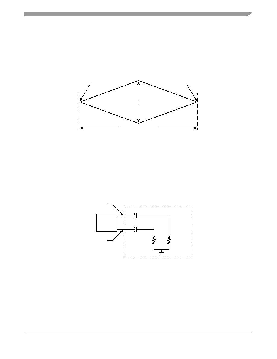
A recovered TX UI is calculated over 3500 consecutive unit intervals of sample data. The eye diagram is created using all edges
of the 250 consecutive UI in the center of the 3500 UI used for calculating the TX UI.
NOTE
The reference impedance for return loss measurements is 50. to ground for both the D+ and
D- line (that is, as measured by a Vector Network Analyzer with 50. probes—see
Figure 71). Note that the series capacitors, CTX, are optional for the return loss
measurement.
Figure 70. Minimum Receiver Eye Timing and Voltage Compliance Specification
2.22.1
Compliance Test and Measurement Load
The AC timing and voltage parameters must be verified at the measurement point, as specified within 0.2 inches of the package
pins, into a test/measurement load shown in the following figure.
NOTE
The allowance of the measurement point to be within 0.2 inches of the package pins is
meant to acknowledge that package/board routing may benefit from D+ and D– not being
exactly matched in length at the package pin boundary.
Figure 71. Compliance Test/Measurement Load
2.23
Clocking
This section describes the PLL configuration of the chip. Note that the platform clock is identical to the core complex bus (CCB)
clock.
VRX-DIFF = 0 mV
(D+, D– Crossing Point
VRX-DIFF = 0 mV
(D+, D– Crossing Point
VRX-DIFFp-p-MIN > 175 mV
0.4 UI = TRX-EYE-MIN
TX
Silicon
+ Package
C = CTX
R = 50
Ω
R = 50
Ω
D+ Package
Pin
D– Package
Pin
D+ Package
Pin
相关PDF资料 |
PDF描述 |
|---|---|
| 395-012-527-201 | CARD EDGE 12POS DL .100X.200 BLK |
| MPC8535AVTAQG | MCU PWRQUICC II 1000MHZ 783-PBGA |
| HFW14R-2STE1LF | CONN FPC/FFC 14POS 1MM R/A SMD |
| 395-012-524-804 | CARD EDGE 12POS DL .100X.200 BLK |
| 395-012-524-802 | CARD EDGE 12POS DL .100X.200 BLK |
相关代理商/技术参数 |
参数描述 |
|---|---|
| MPC8535AVTATHA | 功能描述:微处理器 - MPU 8535 Non E RoHS:否 制造商:Atmel 处理器系列:SAMA5D31 核心:ARM Cortex A5 数据总线宽度:32 bit 最大时钟频率:536 MHz 程序存储器大小:32 KB 数据 RAM 大小:128 KB 接口类型:CAN, Ethernet, LIN, SPI,TWI, UART, USB 工作电源电压:1.8 V to 3.3 V 最大工作温度:+ 85 C 安装风格:SMD/SMT 封装 / 箱体:FBGA-324 |
| MPC8535AVTATLA | 功能描述:微处理器 - MPU 8535 NON E RoHS:否 制造商:Atmel 处理器系列:SAMA5D31 核心:ARM Cortex A5 数据总线宽度:32 bit 最大时钟频率:536 MHz 程序存储器大小:32 KB 数据 RAM 大小:128 KB 接口类型:CAN, Ethernet, LIN, SPI,TWI, UART, USB 工作电源电压:1.8 V to 3.3 V 最大工作温度:+ 85 C 安装风格:SMD/SMT 封装 / 箱体:FBGA-324 |
| MPC8535BVTAKG | 功能描述:微处理器 - MPU 8535 INDUSTRIAL 600 RoHS:否 制造商:Atmel 处理器系列:SAMA5D31 核心:ARM Cortex A5 数据总线宽度:32 bit 最大时钟频率:536 MHz 程序存储器大小:32 KB 数据 RAM 大小:128 KB 接口类型:CAN, Ethernet, LIN, SPI,TWI, UART, USB 工作电源电压:1.8 V to 3.3 V 最大工作温度:+ 85 C 安装风格:SMD/SMT 封装 / 箱体:FBGA-324 |
| MPC8535BVTAKGA | 功能描述:微处理器 - MPU 8535 Non E RoHS:否 制造商:Atmel 处理器系列:SAMA5D31 核心:ARM Cortex A5 数据总线宽度:32 bit 最大时钟频率:536 MHz 程序存储器大小:32 KB 数据 RAM 大小:128 KB 接口类型:CAN, Ethernet, LIN, SPI,TWI, UART, USB 工作电源电压:1.8 V to 3.3 V 最大工作温度:+ 85 C 安装风格:SMD/SMT 封装 / 箱体:FBGA-324 |
| MPC8535BVTANG | 功能描述:微处理器 - MPU 8535 INDUSTRIAL 800 RoHS:否 制造商:Atmel 处理器系列:SAMA5D31 核心:ARM Cortex A5 数据总线宽度:32 bit 最大时钟频率:536 MHz 程序存储器大小:32 KB 数据 RAM 大小:128 KB 接口类型:CAN, Ethernet, LIN, SPI,TWI, UART, USB 工作电源电压:1.8 V to 3.3 V 最大工作温度:+ 85 C 安装风格:SMD/SMT 封装 / 箱体:FBGA-324 |
发布紧急采购,3分钟左右您将得到回复。