- 您现在的位置:买卖IC网 > PDF目录45372 > MPC8567ECVTAUJJA (FREESCALE SEMICONDUCTOR INC) 32-BIT, 1333 MHz, RISC PROCESSOR, PBGA1023 PDF资料下载
参数资料
| 型号: | MPC8567ECVTAUJJA |
| 厂商: | FREESCALE SEMICONDUCTOR INC |
| 元件分类: | 微控制器/微处理器 |
| 英文描述: | 32-BIT, 1333 MHz, RISC PROCESSOR, PBGA1023 |
| 封装: | 33 X 33 MM, 2.75 MM HEIGHT, 1 MM PITCH, LEAD FREE, PLASTIC, FCBGA-1023 |
| 文件页数: | 91/139页 |
| 文件大小: | 1449K |
| 代理商: | MPC8567ECVTAUJJA |
第1页第2页第3页第4页第5页第6页第7页第8页第9页第10页第11页第12页第13页第14页第15页第16页第17页第18页第19页第20页第21页第22页第23页第24页第25页第26页第27页第28页第29页第30页第31页第32页第33页第34页第35页第36页第37页第38页第39页第40页第41页第42页第43页第44页第45页第46页第47页第48页第49页第50页第51页第52页第53页第54页第55页第56页第57页第58页第59页第60页第61页第62页第63页第64页第65页第66页第67页第68页第69页第70页第71页第72页第73页第74页第75页第76页第77页第78页第79页第80页第81页第82页第83页第84页第85页第86页第87页第88页第89页第90页当前第91页第92页第93页第94页第95页第96页第97页第98页第99页第100页第101页第102页第103页第104页第105页第106页第107页第108页第109页第110页第111页第112页第113页第114页第115页第116页第117页第118页第119页第120页第121页第122页第123页第124页第125页第126页第127页第128页第129页第130页第131页第132页第133页第134页第135页第136页第137页第138页第139页
MPC8568E/MPC8567E PowerQUICC III Integrated Processor Hardware Specifications, Rev. 1
Freescale Semiconductor
55
JTAG
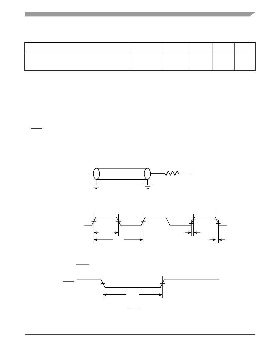
Figure 30 provides the AC test load for TDO and the boundary-scan outputs.
Figure 30. AC Test Load for the JTAG Interface
Figure 31 provides the JTAG clock input timing diagram.
Figure 31. JTAG Clock Input Timing Diagram
Figure 32 provides the TRST timing diagram.
Figure 32. TRST Timing Diagram
JTAG external clock to output high impedance:
Boundary-scan data
TDO
tJTKLDZ
tJTKLOZ
3
19
9
ns
5, 6
Notes:
1. All outputs are measured from the midpoint voltage of the falling/rising edge of tTCLK to the midpoint of the signal in question.
The output timings are measured at the pins. All output timings assume a purely resistive 50-
Ω load (see Figure 30).
Time-of-flight delays must be added for trace lengths, vias, and connectors in the system.
2. The symbols used for timing specifications herein follow the pattern of t(first two letters of functional block)(signal)(state) (reference)(state)
for inputs and t(first two letters of functional block)(reference)(state)(signal)(state) for outputs. For example, tJTDVKH symbolizes JTAG
device timing (JT) with respect to the time data input signals (D) reaching the valid state (V) relative to the tJTG clock reference
(K) going to the high (H) state or setup time. Also, tJTDXKH symbolizes JTAG timing (JT) with respect to the time data input
signals (D) went invalid (X) relative to the tJTG clock reference (K) going to the high (H) state. Note that, in general, the clock
reference symbol representation is based on three letters representing the clock of a particular functional. For rise and fall
times, the latter convention is used with the appropriate letter: R (rise) or F (fall).
3. TRST is an asynchronous level sensitive signal. The setup time is for test purposes only.
4. Non-JTAG signal input timing with respect to tTCLK.
5. Non-JTAG signal output timing with respect to tTCLK.
6. Guaranteed by design
Table 45. JTAG AC Timing Specifications (Independent of SYSCLK) 1 (continued)
At recommended operating conditions (see Table 3).
Parameter
Symbol 2
Min
Max
Unit
Notes
Output
Z0 = 50 Ω
OVDD/2
RL = 50 Ω
JTAG
tJTKHKL
tJTGR
External Clock
VM
tJTG
tJTGF
VM = Midpoint Voltage (OVDD/2)
TRST
VM = Midpoint Voltage (OVDD/2)
VM
tTRST
相关PDF资料 |
PDF描述 |
|---|---|
| MPC8568ECVTAUJJA | 32-BIT, 1333 MHz, RISC PROCESSOR, PBGA1023 |
| MPC8569CVTANKGA | RISC PROCESSOR, PBGA783 |
| MPC8569VTANKGB | RISC PROCESSOR, PBGA783 |
| MPC8569EVTAUNLB | RISC PROCESSOR, PBGA783 |
| MPC8569ECVTANKGB | RISC PROCESSOR, PBGA783 |
相关代理商/技术参数 |
参数描述 |
|---|---|
| MPC8567EPXANGG | 功能描述:微处理器 - MPU 8567 PB Encrypt 800MHz RoHS:否 制造商:Atmel 处理器系列:SAMA5D31 核心:ARM Cortex A5 数据总线宽度:32 bit 最大时钟频率:536 MHz 程序存储器大小:32 KB 数据 RAM 大小:128 KB 接口类型:CAN, Ethernet, LIN, SPI,TWI, UART, USB 工作电源电压:1.8 V to 3.3 V 最大工作温度:+ 85 C 安装风格:SMD/SMT 封装 / 箱体:FBGA-324 |
| MPC8567EPXAQGG | 功能描述:微处理器 - MPU 8567 PB Encrypt 1GHz RoHS:否 制造商:Atmel 处理器系列:SAMA5D31 核心:ARM Cortex A5 数据总线宽度:32 bit 最大时钟频率:536 MHz 程序存储器大小:32 KB 数据 RAM 大小:128 KB 接口类型:CAN, Ethernet, LIN, SPI,TWI, UART, USB 工作电源电压:1.8 V to 3.3 V 最大工作温度:+ 85 C 安装风格:SMD/SMT 封装 / 箱体:FBGA-324 |
| MPC8567EPXAUJJ | 功能描述:微处理器 - MPU 8567 PB Encrypt 1.3GHz RoHS:否 制造商:Atmel 处理器系列:SAMA5D31 核心:ARM Cortex A5 数据总线宽度:32 bit 最大时钟频率:536 MHz 程序存储器大小:32 KB 数据 RAM 大小:128 KB 接口类型:CAN, Ethernet, LIN, SPI,TWI, UART, USB 工作电源电压:1.8 V to 3.3 V 最大工作温度:+ 85 C 安装风格:SMD/SMT 封装 / 箱体:FBGA-324 |
| MPC8567EVTANGG | 功能描述:微处理器 - MPU No PB 800 MHz RoHS:否 制造商:Atmel 处理器系列:SAMA5D31 核心:ARM Cortex A5 数据总线宽度:32 bit 最大时钟频率:536 MHz 程序存储器大小:32 KB 数据 RAM 大小:128 KB 接口类型:CAN, Ethernet, LIN, SPI,TWI, UART, USB 工作电源电压:1.8 V to 3.3 V 最大工作温度:+ 85 C 安装风格:SMD/SMT 封装 / 箱体:FBGA-324 |
| MPC8567EVTAQGG | 功能描述:微处理器 - MPU No PB 1.0 GHz RoHS:否 制造商:Atmel 处理器系列:SAMA5D31 核心:ARM Cortex A5 数据总线宽度:32 bit 最大时钟频率:536 MHz 程序存储器大小:32 KB 数据 RAM 大小:128 KB 接口类型:CAN, Ethernet, LIN, SPI,TWI, UART, USB 工作电源电压:1.8 V to 3.3 V 最大工作温度:+ 85 C 安装风格:SMD/SMT 封装 / 箱体:FBGA-324 |
发布紧急采购,3分钟左右您将得到回复。