- 您现在的位置:买卖IC网 > PDF目录45372 > MPC8569VTAUNLA (FREESCALE SEMICONDUCTOR INC) RISC PROCESSOR, PBGA783 PDF资料下载
参数资料
| 型号: | MPC8569VTAUNLA |
| 厂商: | FREESCALE SEMICONDUCTOR INC |
| 元件分类: | 微控制器/微处理器 |
| 英文描述: | RISC PROCESSOR, PBGA783 |
| 封装: | 29 X 29 MM, 1 MM PITCH, PLASTIC, BGA-783 |
| 文件页数: | 67/126页 |
| 文件大小: | 2847K |
| 代理商: | MPC8569VTAUNLA |
第1页第2页第3页第4页第5页第6页第7页第8页第9页第10页第11页第12页第13页第14页第15页第16页第17页第18页第19页第20页第21页第22页第23页第24页第25页第26页第27页第28页第29页第30页第31页第32页第33页第34页第35页第36页第37页第38页第39页第40页第41页第42页第43页第44页第45页第46页第47页第48页第49页第50页第51页第52页第53页第54页第55页第56页第57页第58页第59页第60页第61页第62页第63页第64页第65页第66页当前第67页第68页第69页第70页第71页第72页第73页第74页第75页第76页第77页第78页第79页第80页第81页第82页第83页第84页第85页第86页第87页第88页第89页第90页第91页第92页第93页第94页第95页第96页第97页第98页第99页第100页第101页第102页第103页第104页第105页第106页第107页第108页第109页第110页第111页第112页第113页第114页第115页第116页第117页第118页第119页第120页第121页第122页第123页第124页第125页第126页
DDR2 and DDR3 SDRAM Controller
MPC8569E PowerQUICC III Integrated Processor Hardware Specifications, Rev. 0
Freescale Semiconductor
45
2.3.2
Real Time Clock Timing
The real time clock timing (RTC) input is sampled by the core complex bus clock (CCB_clk). The output of the sampling latch
is then used as an input to the counters of the PIC and the time base unit of the e500; there is no need for jitter specification.
The minimum pulse width of the RTC signal must be greater than 2x the period of the CCB_clk. That is, minimum clock high
time is 2
× tCCB_clk, and minimum clock low time is 2 × tCCB_clk. There is no minimum RTC frequency; RTC may be grounded
if not needed.
2.3.3
Gigabit Ethernet Reference Clock Timing
The following table provides the gigabit Ethernet reference clock (TX_CLK) AC timing specifications.
2.3.4
Other Input Clocks
A description of the overall clocking of this device is available in the MPC8569E PowerQUICC III Integrated Host Processor
Family Reference Manual in the form of a clock subsystem block diagram. For information about the input clock requirements
of other functional blocks such as SerDes, Ethernet Management, eSDHC, and Enhanced Local Bus see the specific interface
section.
2.4
DDR2 and DDR3 SDRAM Controller
This section describes the DC and AC electrical specifications for the DDR2 and DDR3 SDRAM controller interface of the
MPC8569E. Note that the required GVDD(typ) is 1.8 V for DDR2 SDRAM and GVDD(typ) is 1.5 V for DDR3 SDRAM.
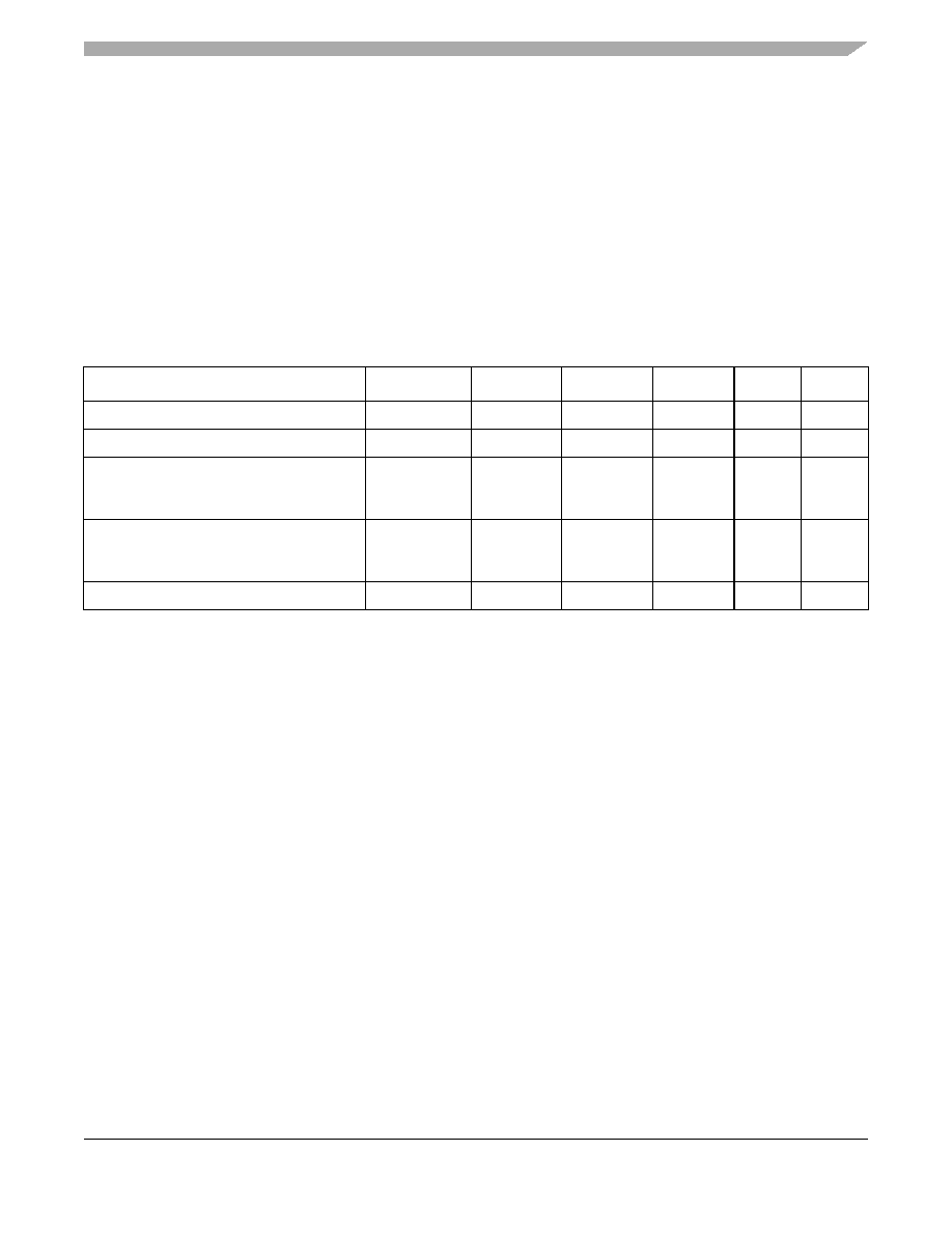
Table 12. TX_CLK3,4 AC Timing Specifications
At recommended operating conditions with LVDD = 2.5 V ± 125 mV / 3.3 V ± 165 mV.
Parameter/Condition
Symbol
Min
Typical
Max
Unit
Notes
TX_CLK frequency
tG125
—125
—
MHz
—
TX_CLK cycle time
tG125
—8
—
ns
—
TX_CLK rise and fall time
LVDD = 2.5 V
LVDD = 3.3 V
tG125R/tG125F
——
0.75
1.0
ns
1, 5
TX_CLK duty cycle
GMII, TBI
1000Base-T for RGMII, RTBI
tG125H/tG125
45
47
—
55
53
%2, 5
TX_CLK jitter
—
± 150
ps
2, 5
Notes:
1. Rise and fall times for TX_CLK are measured from 0.5 and 2.0 V for LVDD = 2.5 V, and from 0.6 and 2.7 V for LVDD =3.3 V.
2. TX_CLK is used to generate the GTX clock for the UEC transmitter with 2% degradation. The TX_CLK duty cycle can be
loosened from 47%/53% as long as the PHY device can tolerate the duty cycle generated by the UEC GTX_CLK. See
Section 2.6.3.7, “RGMII and RTBI AC Timing Specifications,” for duty cycle for 10Base-T and 100Base-T reference clock.
3. Gigabit transmit 125-MHz source. This signal must be generated externally with a crystal or oscillator, or is sometimes
provided by the PHY. TX_CLK is a 125-MHz input into the UCC Ethernet Controller and is used to generate all 125-MHz
related signals and clocks in the following modes: GMII, TBI, RTBI, RGMII.
4. For GMII and TBI modes, TX_CLK is provided to UCC1 through QE_PC[8:11,14,15] (CLK9-12,15,16) and to UCC2 through
QE_PC[2,3,6,7,15:17](CLK3,4,7,8,16:18). For RGMII and RTBI modes, TX_CLK is provided to UCC1 and UCC3 through
QE_PC11(CLK12) and to UCC2 and UCC4 through QE_PC16 (CLK17).
5. System/board must be designed to ensure the input requirement to the device is achieved. Proper device operation is
guaranteed for inputs meeting this requirement by design, simulation, characterization, or functional testing
相关PDF资料 |
PDF描述 |
|---|---|
| MPC8569EVTAUNL | RISC PROCESSOR, PBGA783 |
| MPC8569ECVTAQLJA | RISC PROCESSOR, PBGA783 |
| MPC8569EVTANKGB | RISC PROCESSOR, PBGA783 |
| MPC8569EVTAQLJA | RISC PROCESSOR, PBGA783 |
| MPC8569VTAQLJA | RISC PROCESSOR, PBGA783 |
相关代理商/技术参数 |
参数描述 |
|---|---|
| MPC8569VTAUNLB | 功能描述:数字信号处理器和控制器 - DSP, DSC 8569 ST 1333/667/533 r2.1 RoHS:否 制造商:Microchip Technology 核心:dsPIC 数据总线宽度:16 bit 程序存储器大小:16 KB 数据 RAM 大小:2 KB 最大时钟频率:40 MHz 可编程输入/输出端数量:35 定时器数量:3 设备每秒兆指令数:50 MIPs 工作电源电压:3.3 V 最大工作温度:+ 85 C 封装 / 箱体:TQFP-44 安装风格:SMD/SMT |
| MPC8572CLVTAULD | 功能描述:微处理器 - MPU 1333 LOW PWR EXT TEMP RoHS:否 制造商:Atmel 处理器系列:SAMA5D31 核心:ARM Cortex A5 数据总线宽度:32 bit 最大时钟频率:536 MHz 程序存储器大小:32 KB 数据 RAM 大小:128 KB 接口类型:CAN, Ethernet, LIN, SPI,TWI, UART, USB 工作电源电压:1.8 V to 3.3 V 最大工作温度:+ 85 C 安装风格:SMD/SMT 封装 / 箱体:FBGA-324 |
| MPC8572CLVTAULE | 功能描述:微处理器 - MPU R211 NoE NoPb 1333LP Ext RoHS:否 制造商:Atmel 处理器系列:SAMA5D31 核心:ARM Cortex A5 数据总线宽度:32 bit 最大时钟频率:536 MHz 程序存储器大小:32 KB 数据 RAM 大小:128 KB 接口类型:CAN, Ethernet, LIN, SPI,TWI, UART, USB 工作电源电压:1.8 V to 3.3 V 最大工作温度:+ 85 C 安装风格:SMD/SMT 封装 / 箱体:FBGA-324 |
| MPC8572CLVTAVND | 功能描述:微处理器 - MPU 1500 ExtTmp LwPwr RoHS:否 制造商:Atmel 处理器系列:SAMA5D31 核心:ARM Cortex A5 数据总线宽度:32 bit 最大时钟频率:536 MHz 程序存储器大小:32 KB 数据 RAM 大小:128 KB 接口类型:CAN, Ethernet, LIN, SPI,TWI, UART, USB 工作电源电压:1.8 V to 3.3 V 最大工作温度:+ 85 C 安装风格:SMD/SMT 封装 / 箱体:FBGA-324 |
| MPC8572CLVTAVNE | 功能描述:微处理器 - MPU R211 NoE NoPb 1500LP Ext RoHS:否 制造商:Atmel 处理器系列:SAMA5D31 核心:ARM Cortex A5 数据总线宽度:32 bit 最大时钟频率:536 MHz 程序存储器大小:32 KB 数据 RAM 大小:128 KB 接口类型:CAN, Ethernet, LIN, SPI,TWI, UART, USB 工作电源电压:1.8 V to 3.3 V 最大工作温度:+ 85 C 安装风格:SMD/SMT 封装 / 箱体:FBGA-324 |
发布紧急采购,3分钟左右您将得到回复。