- 您现在的位置:买卖IC网 > PDF目录4068 > MPC859PVR100A (Freescale Semiconductor)IC MPU POWERQUICC 100MHZ 357PBGA PDF资料下载
参数资料
| 型号: | MPC859PVR100A |
| 厂商: | Freescale Semiconductor |
| 文件页数: | 16/96页 |
| 文件大小: | 0K |
| 描述: | IC MPU POWERQUICC 100MHZ 357PBGA |
| 标准包装: | 44 |
| 系列: | MPC8xx |
| 处理器类型: | 32-位 MPC8xx PowerQUICC |
| 速度: | 100MHz |
| 电压: | 1.8V |
| 安装类型: | 表面贴装 |
| 封装/外壳: | 357-BBGA |
| 供应商设备封装: | 357-PBGA(25x25) |
| 包装: | 托盘 |
第1页第2页第3页第4页第5页第6页第7页第8页第9页第10页第11页第12页第13页第14页第15页当前第16页第17页第18页第19页第20页第21页第22页第23页第24页第25页第26页第27页第28页第29页第30页第31页第32页第33页第34页第35页第36页第37页第38页第39页第40页第41页第42页第43页第44页第45页第46页第47页第48页第49页第50页第51页第52页第53页第54页第55页第56页第57页第58页第59页第60页第61页第62页第63页第64页第65页第66页第67页第68页第69页第70页第71页第72页第73页第74页第75页第76页第77页第78页第79页第80页第81页第82页第83页第84页第85页第86页第87页第88页第89页第90页第91页第92页第93页第94页第95页第96页
MPC866/MPC859 Hardware Specifications, Rev. 2
Freescale Semiconductor
23
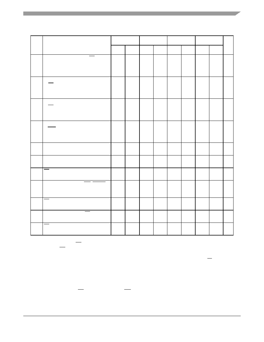
Bus Signal Timing
B35
A(0:31), BADDR(28:30) to CS valid, as
requested by control bit BST4 in the
corresponding word in the UPM (MIN =
0.25 x B1 – 2.00)
5.60
—
4.30
—
3.00
—
1.80
—
ns
B35a A(0:31), BADDR(28:30), and D(0:31)
to BS valid, as Requested by BST1 in
the corresponding word in the UPM
(MIN = 0.50 x B1 – 2.00)
13.20
—
10.50
—
8.00
—
5.60
—
ns
B35b A(0:31), BADDR(28:30), and D(0:31)
to BS valid, as requested by control bit
BST2 in the corresponding word in the
UPM (MIN = 0.75 x B1 – 2.00)
20.70
—
16.70
—
13.00
—
9.40
—
ns
B36
A(0:31), BADDR(28:30), and D(0:31)
to GPL valid as requested by control bit
GxT4 in the corresponding word in the
UPM (MIN = 0.25 x B1 – 2.00)
5.60
—
4.30
—
3.00
—
1.80
—
ns
B37
UPWAIT valid to CLKOUT falling
edge 8 (MIN = 0.00 x B1 + 6.00)
6.00
—
6.00
—
6.00
—
6.00
—
ns
B38
CLKOUT falling edge to UPWAIT
valid8 (MIN = 0.00 x B1 + 1.00)
1.00
—
1.00
—
1.00
—
1.00
—
ns
B39
AS valid to CLKOUT rising edge 9 (MIN
= 0.00 x B1 + 7.00)
7.00
—
7.00
—
7.00
—
7.00
—
ns
B40
A(0:31), TSIZ(0:1), RD/WR, BURST,
valid to CLKOUT rising edge (MIN =
0.00 x B1 + 7.00)
7.00
—
7.00
—
7.00
—
7.00
—
ns
B41
TS valid to CLKOUT rising edge (setup
time) (MIN = 0.00 x B1 + 7.00)
7.00
—
7.00
—
7.00
—
7.00
—
ns
B42
CLKOUT rising edge to TS valid (hold
time) (MIN = 0.00 x B1 + 2.00)
2.00
—
2.00
—
2.00
—
2.00
—
ns
B43
AS negation to memory controller
signals negation (MAX = TBD)
—
TBD
—
TBD
—
TBD
—
TBD
ns
1
For part speeds above 50 MHz, use 9.80 ns for B11a.
2
The timing required for BR input is relevant when the MPC866/859 is selected to work with the internal bus arbiter.
The timing for BG input is relevant when the MPC866/859 is selected to work with the external bus arbiter.
3
For part speeds above 50 MHz, use 2 ns for B17.
4
The D(0:31) and DP(0:3) input timings B18 and B19 refer to the rising edge of CLKOUT, in which the TA input signal
is asserted.
5
For part speeds above 50 MHz, use 2 ns for B19.
6
The D(0:31) and DP(0:3) input timings B20 and B21 refer to the falling edge of CLKOUT. This timing is valid only for
read accesses controlled by chip-selects under control of the UPM in the memory controller, for data beats, where
DLT3 = 1 in the UPM RAM words. (This is only the case where data is latched on the falling edge of CLKOUT.)
7
The timing B30 refers to CS when ACS = 00 and to WE(0:3) when CSNT = 0.
Table 9. Bus Operation Timings (continued)
Num
Characteristic
33 MHz
40 MHz
50 MHz
66 MHz
Unit
Min
Max
Min
Max
Min
Max
Min
Max
相关PDF资料 |
PDF描述 |
|---|---|
| XF2L-2125-1A | CONN FPC 21POS 0.5MM SMT |
| IDT71V67703S80BGGI | IC SRAM 9MBIT 80NS 119BGA |
| MPC859PZP100A | IC MPU POWERQUICC 100MHZ 357PBGA |
| MPC8358VVADDEA | IC MPU POWERQUICC II PRO 740TBGA |
| IDT71V67703S75BGGI | IC SRAM 9MBIT 75NS 119BGA |
相关代理商/技术参数 |
参数描述 |
|---|---|
| MPC859PVR133A | 功能描述:微处理器 - MPU PQ I HIP6W NO-PB RoHS:否 制造商:Atmel 处理器系列:SAMA5D31 核心:ARM Cortex A5 数据总线宽度:32 bit 最大时钟频率:536 MHz 程序存储器大小:32 KB 数据 RAM 大小:128 KB 接口类型:CAN, Ethernet, LIN, SPI,TWI, UART, USB 工作电源电压:1.8 V to 3.3 V 最大工作温度:+ 85 C 安装风格:SMD/SMT 封装 / 箱体:FBGA-324 |
| MPC859PZP100A | 功能描述:微处理器 - MPU POWER QUICC I HIP6W RoHS:否 制造商:Atmel 处理器系列:SAMA5D31 核心:ARM Cortex A5 数据总线宽度:32 bit 最大时钟频率:536 MHz 程序存储器大小:32 KB 数据 RAM 大小:128 KB 接口类型:CAN, Ethernet, LIN, SPI,TWI, UART, USB 工作电源电压:1.8 V to 3.3 V 最大工作温度:+ 85 C 安装风格:SMD/SMT 封装 / 箱体:FBGA-324 |
| MPC859PZP133A | 功能描述:微处理器 - MPU POWER QUICC I HIP6W RoHS:否 制造商:Atmel 处理器系列:SAMA5D31 核心:ARM Cortex A5 数据总线宽度:32 bit 最大时钟频率:536 MHz 程序存储器大小:32 KB 数据 RAM 大小:128 KB 接口类型:CAN, Ethernet, LIN, SPI,TWI, UART, USB 工作电源电压:1.8 V to 3.3 V 最大工作温度:+ 85 C 安装风格:SMD/SMT 封装 / 箱体:FBGA-324 |
| MPC859TCVR100A | 功能描述:微处理器 - MPU PQ I HIP6W NO-PB RoHS:否 制造商:Atmel 处理器系列:SAMA5D31 核心:ARM Cortex A5 数据总线宽度:32 bit 最大时钟频率:536 MHz 程序存储器大小:32 KB 数据 RAM 大小:128 KB 接口类型:CAN, Ethernet, LIN, SPI,TWI, UART, USB 工作电源电压:1.8 V to 3.3 V 最大工作温度:+ 85 C 安装风格:SMD/SMT 封装 / 箱体:FBGA-324 |
| MPC859TCZP100A | 功能描述:微处理器 - MPU POWER QUICC I HIP6W RoHS:否 制造商:Atmel 处理器系列:SAMA5D31 核心:ARM Cortex A5 数据总线宽度:32 bit 最大时钟频率:536 MHz 程序存储器大小:32 KB 数据 RAM 大小:128 KB 接口类型:CAN, Ethernet, LIN, SPI,TWI, UART, USB 工作电源电压:1.8 V to 3.3 V 最大工作温度:+ 85 C 安装风格:SMD/SMT 封装 / 箱体:FBGA-324 |
发布紧急采购,3分钟左右您将得到回复。