- 您现在的位置:买卖IC网 > PDF目录4106 > MPC885VR66 (Freescale Semiconductor)IC MPU POWERQUICC 66MHZ 357PBGA PDF资料下载
参数资料
| 型号: | MPC885VR66 |
| 厂商: | Freescale Semiconductor |
| 文件页数: | 16/87页 |
| 文件大小: | 0K |
| 描述: | IC MPU POWERQUICC 66MHZ 357PBGA |
| 标准包装: | 44 |
| 系列: | MPC8xx |
| 处理器类型: | 32-位 MPC8xx PowerQUICC |
| 速度: | 66MHz |
| 电压: | 3.3V |
| 安装类型: | 表面贴装 |
| 封装/外壳: | 357-BBGA |
| 供应商设备封装: | 357-PBGA(25x25) |
| 包装: | 托盘 |
第1页第2页第3页第4页第5页第6页第7页第8页第9页第10页第11页第12页第13页第14页第15页当前第16页第17页第18页第19页第20页第21页第22页第23页第24页第25页第26页第27页第28页第29页第30页第31页第32页第33页第34页第35页第36页第37页第38页第39页第40页第41页第42页第43页第44页第45页第46页第47页第48页第49页第50页第51页第52页第53页第54页第55页第56页第57页第58页第59页第60页第61页第62页第63页第64页第65页第66页第67页第68页第69页第70页第71页第72页第73页第74页第75页第76页第77页第78页第79页第80页第81页第82页第83页第84页第85页第86页第87页
MPC885/MPC880 PowerQUICC Hardware Specifications, Rev. 7
Freescale Semiconductor
23
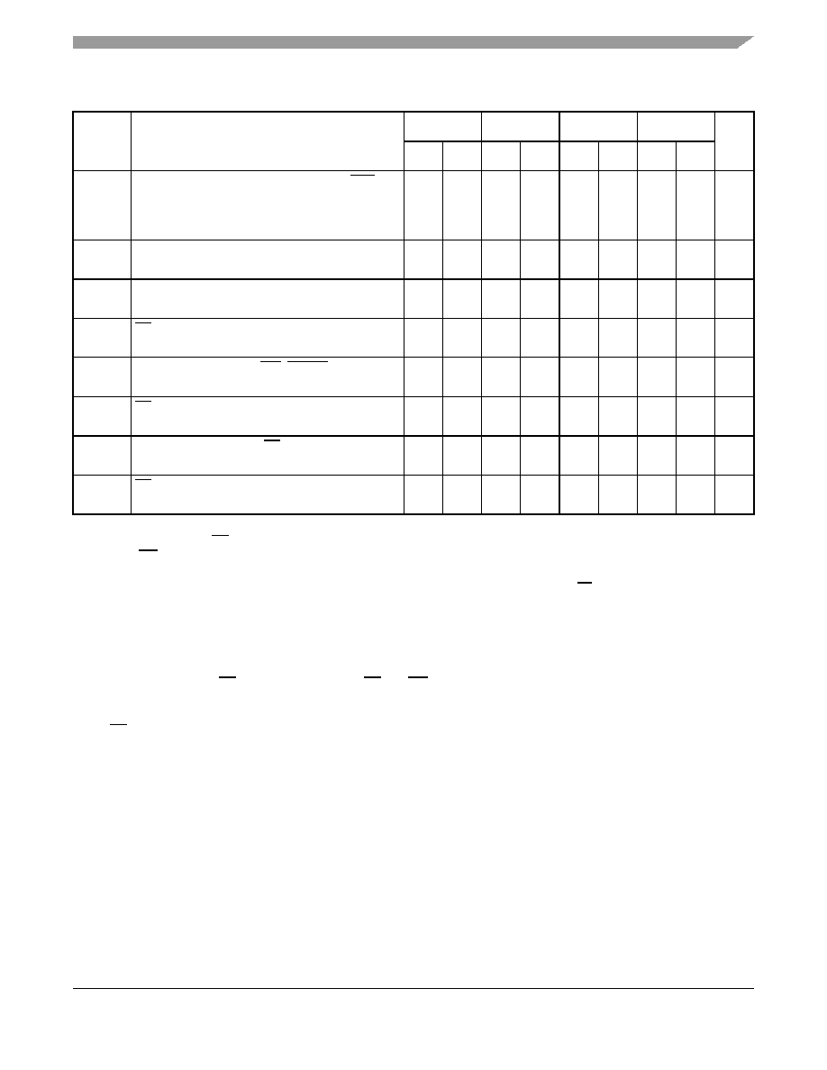
Bus Signal Timing
B36
A(0:31), BADDR(28:30), and D(0:31) to GPL
valid, as requested by control bit GxT4 in the
corresponding word in the UPM
(MIN = 0.25
× B1 – 2.00)
5.60
—
4.30
—
1.80
—
1.13
—
ns
B37
UPWAIT valid to CLKOUT falling edge9
(MIN = 0.00
× B1 + 6.00)
6.00
—
6.00
—
6.00
—
6.00
—
ns
B38
CLKOUT falling edge to UPWAIT valid 9
(MIN = 0.00
× B1 + 1.00)
1.00
—
1.00
—
1.00
—
1.00
—
ns
B39
AS valid to CLKOUT rising edge10
(MIN = 0.00
× B1 + 7.00)
7.00
—
7.00
—
7.00
—
7.00
—
ns
B40
A(0:31), TSIZ(0:1), RD/WR, BURST, valid to
CLKOUT rising edge (MIN = 0.00
× B1 + 7.00)
7.00
—
7.00
—
7.00
—
7.00
—
ns
B41
TS valid to CLKOUT rising edge (setup time)
(MIN = 0.00
× B1 + 7.00)
7.00
—
7.00
—
7.00
—
7.00
—
ns
B42
CLKOUT rising edge to TS valid (hold time)
(MIN = 0.00
× B1 + 2.00)
2.00
—
2.00
—
2.00
—
2.00
—
ns
B43
AS negation to memory controller signals
negation (MAX = TBD)
—TBD
ns
1 For part speeds above 50 MHz, use 9.80 ns for B11a.
2 The timing required for BR input is relevant when the MPC885/MPC880 is selected to work with the internal bus arbiter. The
timing for BG input is relevant when the MPC885/MPC880 is selected to work with the external bus arbiter.
3 For part speeds above 50 MHz, use 2 ns for B17.
4 The D(0:31) input timings B18 and B19 refer to the rising edge of the CLKOUT in which the TA input signal is asserted.
5 For part speeds above 50 MHz, use 2 ns for B19.
6 The D(0:31) input timings B20 and B21 refer to the falling edge of the CLKOUT. This timing is valid only for read accesses
controlled by chip-selects under control of the user-programmable machine (UPM) in the memory controller, for data beats
where DLT3 = 1 in the RAM words. (This is only the case where data is latched on the falling edge of CLKOUT.)
7 This formula applies to bus operation up to 50 MHz.
8 The timing B30 refers to CS when ACS = 00 and to CS and WE(0:3) when CSNT = 0.
9 The signal UPWAIT is considered asynchronous to the CLKOUT and synchronized internally. The timings specified in B37 and
B38 are specified to enable the freeze of the UPM output signals as described in Figure 21.
10 The AS signal is considered asynchronous to the CLKOUT. The timing B39 is specified in order to allow the behavior specified
in Figure 24.
Table 9. Bus Operation Timings (continued)
Num
Characteristic
33 MHz
40 MHz
66 MHz
80 MHz
Unit
Min
Max
Min
Max
Min
Max
Min
Max
相关PDF资料 |
PDF描述 |
|---|---|
| IDT7143SA35PF8 | IC SRAM 32KBIT 35NS 100TQFP |
| IDT7133SA35PF8 | IC SRAM 32KBIT 35NS 100TQFP |
| IDT71V30L25TFG | IC SRAM 8KBIT 25NS 64TQFP |
| IDT71V30L25TF | IC SRAM 8KBIT 25NS 64TQFP |
| ATF16LV8C-10XU | IC PLD 10NS 20TSSOP |
相关代理商/技术参数 |
参数描述 |
|---|---|
| MPC885VR80 | 功能描述:微处理器 - MPU PQ I HIP6W DUET RoHS:否 制造商:Atmel 处理器系列:SAMA5D31 核心:ARM Cortex A5 数据总线宽度:32 bit 最大时钟频率:536 MHz 程序存储器大小:32 KB 数据 RAM 大小:128 KB 接口类型:CAN, Ethernet, LIN, SPI,TWI, UART, USB 工作电源电压:1.8 V to 3.3 V 最大工作温度:+ 85 C 安装风格:SMD/SMT 封装 / 箱体:FBGA-324 |
| MPC885ZP133 | 功能描述:微处理器 - MPU PQ I HIP6W DUET RoHS:否 制造商:Atmel 处理器系列:SAMA5D31 核心:ARM Cortex A5 数据总线宽度:32 bit 最大时钟频率:536 MHz 程序存储器大小:32 KB 数据 RAM 大小:128 KB 接口类型:CAN, Ethernet, LIN, SPI,TWI, UART, USB 工作电源电压:1.8 V to 3.3 V 最大工作温度:+ 85 C 安装风格:SMD/SMT 封装 / 箱体:FBGA-324 |
| MPC885ZP66 | 功能描述:微处理器 - MPU PQ I HIP6W DUET RoHS:否 制造商:Atmel 处理器系列:SAMA5D31 核心:ARM Cortex A5 数据总线宽度:32 bit 最大时钟频率:536 MHz 程序存储器大小:32 KB 数据 RAM 大小:128 KB 接口类型:CAN, Ethernet, LIN, SPI,TWI, UART, USB 工作电源电压:1.8 V to 3.3 V 最大工作温度:+ 85 C 安装风格:SMD/SMT 封装 / 箱体:FBGA-324 |
| MPC885ZP80 | 功能描述:微处理器 - MPU PQ I HIP6W DUET RoHS:否 制造商:Atmel 处理器系列:SAMA5D31 核心:ARM Cortex A5 数据总线宽度:32 bit 最大时钟频率:536 MHz 程序存储器大小:32 KB 数据 RAM 大小:128 KB 接口类型:CAN, Ethernet, LIN, SPI,TWI, UART, USB 工作电源电压:1.8 V to 3.3 V 最大工作温度:+ 85 C 安装风格:SMD/SMT 封装 / 箱体:FBGA-324 |
| MPC-8890 | 制造商:AAEON 制造商全称:AAEON 功能描述:Intel Pentium M or Celeron M Processors |
发布紧急采购,3分钟左右您将得到回复。