- 您现在的位置:买卖IC网 > PDF目录80349 > MPC905D (MOTOROLA INC) 50 MHz, PROC SPECIFIC CLOCK GENERATOR, PDSO16 PDF资料下载
参数资料
| 型号: | MPC905D |
| 厂商: | MOTOROLA INC |
| 元件分类: | 时钟产生/分配 |
| 英文描述: | 50 MHz, PROC SPECIFIC CLOCK GENERATOR, PDSO16 |
| 封装: | PLASTIC, SOIC-16 |
| 文件页数: | 1/5页 |
| 文件大小: | 92K |
| 代理商: | MPC905D |
6
MOTOROLA
SEMICONDUCTOR TECHNICAL DATA
Order this document
by MPC905/D
MOTOROLA ADVANCED CLOCK DRIVERS DEVICE DATA
528
1:6 PCI Clock Generator/
Fanout Buffer
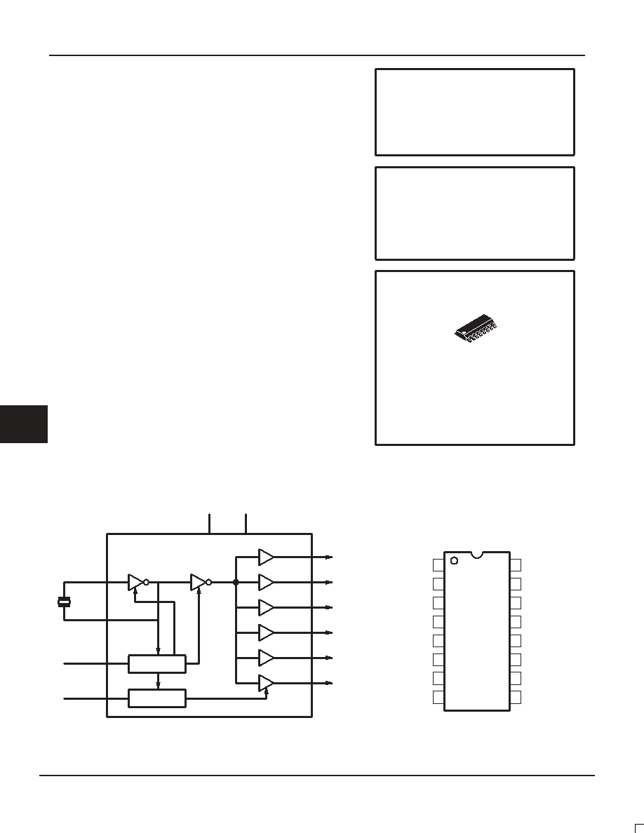
The MPC905 is a six output clock generation device targeted to pro-
vide the clocks required in a 3.3V or 5.0V PCI environment. The device
operates from a 3.3V supply and can interface to either a TTL input or an
external crystal. The inputs to the device can be driven with 5.0V when
the VCC is at 3.3V. The outputs of the MPC905 meet all of the specifica-
tions of the PCI standard.
Six Low Skew Outputs
Synchronous Output Enables for Power Management
Low Voltage Operation
XTAL Oscillator Interface
16-Lead SOIC Package
5.0V Tolerant Enable Inputs
The MPC905 device is targeted for PCI bus or processor bus environ-
ments with up to 12 clock loads. Each of the six outputs on the MPC905
can drive two series terminated 50
transmission lines. This capability
effectively makes the MPC905 a 1:12 fanout buffer.
The MPC905 offers two synchronous enable inputs to allow users flex-
ibility in developing power management features for their designs. Both
enable signals are active HIGH inputs. A logic ‘0’ on the Enable1 will pull
outputs 0 to 4 into the logic ‘0’ state. A logic ‘1’ on the Enable1 input will
result in outputs 0 to 4 to be toggling. A logic ‘0’ on Enable2 will cause
output BLK5 to a logic ‘0’ state, whereas a logic ‘1’ on Enable2 will cause
output BLK5 to toggle. The oscillator remains on.
The Enable2 input can be used to disable any high power device for system power savings during periods of inactivity. Both
enable inputs are synchronized internal to the chip so that the output disabling will happen only when the outputs are already
LOW. This feature guarantees no runt pulses will be generated during enabling and disabling.
BCLK0
BCLK1
BCLK2
BCLK3
BCLK4
BCLK5
XTAL_IN
XTAL_OUT
Enable1
Enable2
GND (3)
VDD (3)
Pinout: 16-Lead Plastic Package (Top View)
16
1
15
2
14
3
13
4
XTAL_IN
Enable1
BCLK5
VDD3
XTAL_OUT
Enable2
GND1
BCLK0
12
5
11
6
10
7
9
8
BCLK4
GND3
BCLK3
VDD2
VDD1
BCLK1
GND2
BCLK2
SYNCHRONIZE
Rev 2
1:6 PCI
CLOCK GENERATOR/
FANOUT BUFFER
D SUFFIX
PLASTIC SOIC PACKAGE
CASE 751B
1
16
MPC905
相关PDF资料 |
PDF描述 |
|---|---|
| MCIMX257CJM4A | 32-BIT, 400 MHz, MICROPROCESSOR, PBGA400 |
| M102P0200.0000CK | 200 MHz, OTHER CLOCK GENERATOR, MDIP24 |
| MC3S12XEP100F1CVLR | 32-BIT, FLASH, 50 MHz, RISC MICROCONTROLLER, PBGA208 |
| MPC8541CPXAPFX | 32-BIT, 1420 MHz, RISC PROCESSOR, CBGA360 |
| MPC8541ECVTAPDX | 32-BIT, 1700 MHz, RISC PROCESSOR, CBGA360 |
相关代理商/技术参数 |
参数描述 |
|---|---|
| MPC905DR2 | 功能描述:IC CLK BUFFER 1:6 100MHZ 16-SOIC RoHS:否 类别:集成电路 (IC) >> 时钟/计时 - 时钟缓冲器,驱动器 系列:- 标准包装:1 系列:HiPerClockS™ 类型:扇出缓冲器(分配),多路复用器 电路数:1 比率 - 输入:输出:2:18 差分 - 输入:输出:是/无 输入:CML,LVCMOS,LVPECL,LVTTL,SSTL 输出:LVCMOS,LVTTL 频率 - 最大:250MHz 电源电压:2.375 V ~ 3.465 V 工作温度:0°C ~ 70°C 安装类型:表面贴装 封装/外壳:32-LQFP 供应商设备封装:32-TQFP(7x7) 包装:- 其它名称:800-1923-6 |
| MPC905EF | 功能描述:时钟缓冲器 FSL 1-6 PCI Clock Gen./Fanout Buffer RoHS:否 制造商:Texas Instruments 输出端数量:5 最大输入频率:40 MHz 传播延迟(最大值): 电源电压-最大:3.45 V 电源电压-最小:2.375 V 最大功率耗散: 最大工作温度:+ 85 C 最小工作温度:- 40 C 封装 / 箱体:LLP-24 封装:Reel |
| MPC905EFR2 | 功能描述:时钟发生器及支持产品 FSL 1-6 PCI Clock Gen./Fanout Buffer RoHS:否 制造商:Silicon Labs 类型:Clock Generators 最大输入频率:14.318 MHz 最大输出频率:166 MHz 输出端数量:16 占空比 - 最大:55 % 工作电源电压:3.3 V 工作电源电流:1 mA 最大工作温度:+ 85 C 安装风格:SMD/SMT 封装 / 箱体:QFN-56 |
| MPC909 | 制造商:MOTOROLA 制造商全称:Motorola, Inc 功能描述:LOW VOLTAGE CMOS 1:18 CLOCK DISTRIBUTION CHIP |
| MPC9100 | 制造商:MOTOROLA 制造商全称:Motorola, Inc 功能描述:DUAL PLL CLOCK GENERATOR |
发布紧急采购,3分钟左右您将得到回复。