- 您现在的位置:买卖IC网 > PDF目录80364 > MPC905DR2 (FREESCALE SEMICONDUCTOR INC) 50 MHz, PROC SPECIFIC CLOCK GENERATOR, PDSO16 PDF资料下载
参数资料
| 型号: | MPC905DR2 |
| 厂商: | FREESCALE SEMICONDUCTOR INC |
| 元件分类: | 时钟产生/分配 |
| 英文描述: | 50 MHz, PROC SPECIFIC CLOCK GENERATOR, PDSO16 |
| 封装: | PLASTIC, SOIC-16 |
| 文件页数: | 4/5页 |
| 文件大小: | 92K |
| 代理商: | MPC905DR2 |
6
MPC905
MOTOROLA ADVANCED CLOCK DRIVERS DEVICE DATA
531
BCLK0-4
BCLK5
ENABLE2
ENABLE1
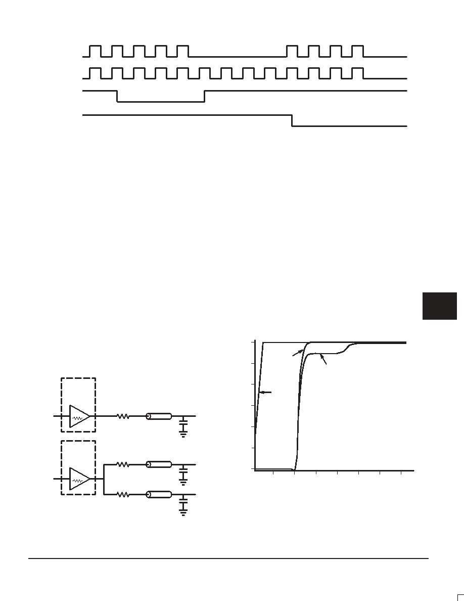
Figure 3. Enable Timing Diagram
APPLICATIONS INFORMATION
Driving Transmission Lines
The MPC905 clock driver was designed to drive high speed
signals in a terminated transmission line environment. To pro-
vide the optimum flexibility to the user the output drivers were
designed to exhibit the lowest impedance possible. With an
output impedance of approximately 10
the drivers can drive
either parallel or series terminated transmission lines. For
more information on transmission lines the reader is referred to
application note AN1091 in the Timing Solutions data book
(DL207/D).
In most high performance clock networks point–to–point
distribution of signals is the method of choice. In a point–to–
point scheme either series terminated or parallel terminated
transmission lines can be used. The parallel technique termi-
nates the signal at the end of the line with a 50
resistance to
VCC/2. This technique draws a fairly high level of DC current
and thus only a single terminated line can be driven by each
output of the MPC905 clock driver. For the series terminated
case however there is no DC current draw, thus the outputs
can drive multiple series terminated lines. Figure 4 illustrates
an output driving a single series terminated line vs two series
terminated lines in parallel. When taken to its extreme the fan-
out of the MPC905 clock driver is effectively doubled due to its
capability to drive multiple lines.
Figure 4. Single versus Dual Transmission Lines
10
IN
MPC905
OUTPUT
BUFFER
RS = 40
ZO = 50
OutA
10W
IN
MPC905
OUTPUT
BUFFER
RS = 40
ZO = 50
OutB0
RS = 40
ZO = 50
OutB1
The waveform plots of Figure 5 show the simulation results
of an output driving a single line vs two lines. In both cases the
drive capability of the MPC905 output buffers is more than suf-
ficient to drive 50
transmission lines on the incident edge.
Note from the delay measurements in the simulations a delta
of only 43ps exists between the two differently loaded outputs.
The output waveform in Figure 5 shows a step in the wave-
form, this step is caused by the impedance mismatch seen
looking into the driver. The parallel combination of the 40
se-
ries resistor plus the output impedance does not match the
parallel combination of the line impedances. The voltage wave
launched down the two lines will equal:
VL = VS ( Zo / Rs + Ro +Zo) = 3.0 (25/55) = 1.36V
At the load end the voltage will double, due to the near unity
reflection coefficient, to 2.73V. It will then increment towards
the quiescent 3.0V in steps separated by one round trip delay
(in this case 4.0ns).
Figure 5. Single versus Dual Waveforms
TIME (nS)
VOL
TAGE
(V)
3.0
2.5
2.0
1.5
1.0
0.5
0
2
4
6
8
10
12
14
OutB
tD = 3.9386
OutA
tD = 3.8956
In
相关PDF资料 |
PDF描述 |
|---|---|
| MC68HC05JP6CDW | 8-BIT, MROM, 2.1 MHz, MICROCONTROLLER, PDSO28 |
| MC9S12C96CPB25 | 16-BIT, FLASH, 25 MHz, MICROCONTROLLER, PQFP52 |
| MC9S12C96PMPB16 | 16-BIT, FLASH, 16 MHz, MICROCONTROLLER, PQFP52 |
| MC9S12GC16PMFU25 | 16-BIT, FLASH, 25 MHz, MICROCONTROLLER, PQFP80 |
| MC9S12GC64CPB25 | 16-BIT, FLASH, 25 MHz, MICROCONTROLLER, PQFP52 |
相关代理商/技术参数 |
参数描述 |
|---|---|
| MPC905EF | 功能描述:时钟缓冲器 FSL 1-6 PCI Clock Gen./Fanout Buffer RoHS:否 制造商:Texas Instruments 输出端数量:5 最大输入频率:40 MHz 传播延迟(最大值): 电源电压-最大:3.45 V 电源电压-最小:2.375 V 最大功率耗散: 最大工作温度:+ 85 C 最小工作温度:- 40 C 封装 / 箱体:LLP-24 封装:Reel |
| MPC905EFR2 | 功能描述:时钟发生器及支持产品 FSL 1-6 PCI Clock Gen./Fanout Buffer RoHS:否 制造商:Silicon Labs 类型:Clock Generators 最大输入频率:14.318 MHz 最大输出频率:166 MHz 输出端数量:16 占空比 - 最大:55 % 工作电源电压:3.3 V 工作电源电流:1 mA 最大工作温度:+ 85 C 安装风格:SMD/SMT 封装 / 箱体:QFN-56 |
| MPC909 | 制造商:MOTOROLA 制造商全称:Motorola, Inc 功能描述:LOW VOLTAGE CMOS 1:18 CLOCK DISTRIBUTION CHIP |
| MPC9100 | 制造商:MOTOROLA 制造商全称:Motorola, Inc 功能描述:DUAL PLL CLOCK GENERATOR |
| MPC9108 | 制造商:MOTOROLA 制造商全称:Motorola, Inc 功能描述:MULTIPLE OUTPUT CLOCK SYNTHESIZER |
发布紧急采购,3分钟左右您将得到回复。