- 您现在的位置:买卖IC网 > PDF目录9004 > MPC9239AC (IDT, Integrated Device Technology Inc)IC CLK SYNTH LV PECL 32-LQFP PDF资料下载
参数资料
| 型号: | MPC9239AC |
| 厂商: | IDT, Integrated Device Technology Inc |
| 文件页数: | 4/10页 |
| 文件大小: | 0K |
| 描述: | IC CLK SYNTH LV PECL 32-LQFP |
| 标准包装: | 250 |
| 类型: | 时钟/频率合成器 |
| PLL: | 是 |
| 输入: | 晶体 |
| 输出: | LVPECL |
| 电路数: | 1 |
| 比率 - 输入:输出: | 1:1 |
| 差分 - 输入:输出: | 无/是 |
| 频率 - 最大: | 900MHz |
| 除法器/乘法器: | 是/无 |
| 电源电压: | 3.135 V ~ 3.465 V |
| 工作温度: | 0°C ~ 70°C |
| 安装类型: | 表面贴装 |
| 封装/外壳: | 32-LQFP |
| 供应商设备封装: | 32-TQFP(7x7) |
| 包装: | 托盘 |
MPC9239
REVISION 2
DECEMBER 18, 2012
3
2012 Integrated Device Technology, Inc.
MPC9239 Data Sheet
900 MHz Low Voltage LVPECL Clock Synthesizer
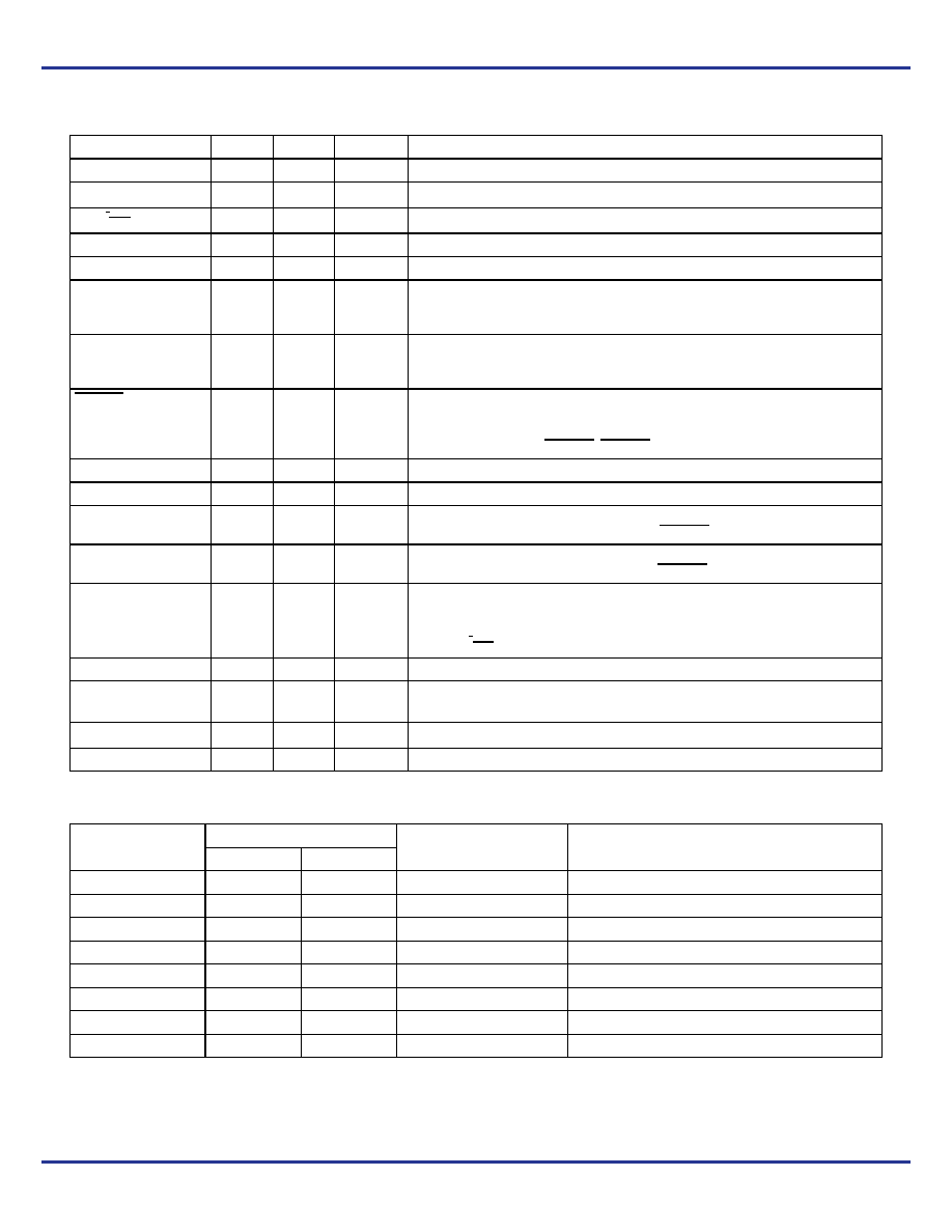
Table 1. Pin Configurations
Pin
I/O
Default
Type
Function
XTAL_IN, XTAL_OUT
Analog
Crystal oscillator interface.
fREF_EXT
Input
0
LVCMOS Alternative PLL reference input.
fOUT, fOUT
Output
LVPECL
Differential clock output.
TEST
Output
LVCMOS Test and device diagnosis output.
XTAL_SEL
Input
1
LVCMOS PLL reference select input.
PWR_DOWN
Input
0
LVCMOS Configuration input for power down mode. Assertion (deassertion) of power down will
decrease (increase) the output frequency by a ratio of 16 in 4 discrete steps.
PWR_DOWN assertion (deassertion) is synchronous to the input reference clock.
S_LOAD
Input
0
LVCMOS Serial configuration control input. This inputs controls the loading of the configuration
latches with the contents of the shift register. The latches will be transparent when this
signal is high, thus the data must be stable on the high-to-low transition.
P_LOAD
Input
1
LVCMOS Parallel configuration control input. this input controls the loading of the configuration
latches with the content of the parallel inputs (M and N). The latches will be
transparent when this signal is low, thus the parallel data must be stable on the
low-to-high transition of P_LOAD. P_LOAD is state sensitive.
S_DATA
Input
0
LVCMOS Serial configuration data input.
S_CLOCK
Input
0
LVCMOS Serial configuration clock input.
M[0:6]
Input
1
LVCMOS Parallel configuration for PLL feedback divider (M).
M is sampled on the low-to-high transition of P_LOAD.
N[1:0]
Input
1
LVCMOS Parallel configuration for Post-PLL divider (N).
N is sampled on the low-to-high transition of P_LOAD.
OE
Input
1
LVCMOS Output enable (active high).
The output enable is synchronous to the output clock to eliminate the possibility of runt
pulses on the fOUT output. OE = L low stops fOUT in the logic low stat
(fOUT = L, fOUT =H).
GND
Supply
Ground
Negative power supply (GND).
VCC
Supply
VCC
Positive power supply for I/O and core. All VCC pins must be connected to the positive
power supply for correct operation.
VCC_PLL
Supply
VCC
PLL positive power supply (analog power supply).
NC
Do not connect.
Table 2. Output Frequency Range and PLL Post-Divider N
PWR_DOWN
N
VCO Output Frequency
Division
fOUT Frequency Range
1
0
0
2
200 – 450 MHz
0
1
4
100 – 225 MHz
0
1
0
8
50 – 112.5 MHz
0
1
400 – 900 MHz
1
0
32
12.5 – 28.125 MHz
1
0
1
64
6.25 – 14.0625 MHz
1
0
128
3.125 – 7.03125 MHz
1
16
25 – 56.25 MHz
相关PDF资料 |
PDF描述 |
|---|---|
| VE-BN1-MV-F3 | CONVERTER MOD DC/DC 12V 150W |
| MK2772-01SLF | IC CLK SRC VCXO/SET-TOP 20-SOIC |
| VE-BN1-MV-F1 | CONVERTER MOD DC/DC 12V 150W |
| VE-BN0-MV-F3 | CONVERTER MOD DC/DC 5V 150W |
| VE-BN0-MV-F2 | CONVERTER MOD DC/DC 5V 150W |
相关代理商/技术参数 |
参数描述 |
|---|---|
| MPC9239ACR2 | 功能描述:时钟合成器/抖动清除器 RoHS:否 制造商:Skyworks Solutions, Inc. 输出端数量: 输出电平: 最大输出频率: 输入电平: 最大输入频率:6.1 GHz 电源电压-最大:3.3 V 电源电压-最小:2.7 V 封装 / 箱体:TSSOP-28 封装:Reel |
| MPC9239EI | 功能描述:时钟合成器/抖动清除器 FSL 900MHz LVPECL Freq. Synthesizer RoHS:否 制造商:Skyworks Solutions, Inc. 输出端数量: 输出电平: 最大输出频率: 输入电平: 最大输入频率:6.1 GHz 电源电压-最大:3.3 V 电源电压-最小:2.7 V 封装 / 箱体:TSSOP-28 封装:Reel |
| MPC9239EIR2 | 功能描述:时钟合成器/抖动清除器 RoHS:否 制造商:Skyworks Solutions, Inc. 输出端数量: 输出电平: 最大输出频率: 输入电平: 最大输入频率:6.1 GHz 电源电压-最大:3.3 V 电源电压-最小:2.7 V 封装 / 箱体:TSSOP-28 封装:Reel |
| MPC9239FA | 功能描述:时钟合成器/抖动清除器 3.3V 900MHz Clock Generator RoHS:否 制造商:Skyworks Solutions, Inc. 输出端数量: 输出电平: 最大输出频率: 输入电平: 最大输入频率:6.1 GHz 电源电压-最大:3.3 V 电源电压-最小:2.7 V 封装 / 箱体:TSSOP-28 封装:Reel |
| MPC9239FN | 功能描述:IC PECL CLOCK LV 900MHZ 28-PLCC RoHS:否 类别:集成电路 (IC) >> 时钟/计时 - 时钟发生器,PLL,频率合成器 系列:- 标准包装:39 系列:- 类型:* PLL:带旁路 输入:时钟 输出:时钟 电路数:1 比率 - 输入:输出:1:10 差分 - 输入:输出:是/是 频率 - 最大:170MHz 除法器/乘法器:无/无 电源电压:2.375 V ~ 3.465 V 工作温度:0°C ~ 70°C 安装类型:* 封装/外壳:* 供应商设备封装:* 包装:* |
发布紧急采购,3分钟左右您将得到回复。