- 您现在的位置:买卖IC网 > PDF目录80499 > MPC92439FNR2 (INTEGRATED DEVICE TECHNOLOGY INC) 900 MHz, OTHER CLOCK GENERATOR, PQCC28 PDF资料下载
参数资料
| 型号: | MPC92439FNR2 |
| 厂商: | INTEGRATED DEVICE TECHNOLOGY INC |
| 元件分类: | 时钟产生/分配 |
| 英文描述: | 900 MHz, OTHER CLOCK GENERATOR, PQCC28 |
| 封装: | PLASTIC, LCC-28 |
| 文件页数: | 1/16页 |
| 文件大小: | 288K |
| 代理商: | MPC92439FNR2 |
MPC92439
Rev 2, 05/2005
Freescale Semiconductor
Technical Data
Freescale Semiconductor, Inc., 2005. All rights reserved.
900 MHz Low Voltage
LVPECL Clock Synthesizer
The MPC92439 is a 3.3 V compatible, PLL based clock synthesizer targeted
for high performance clock generation in mid-range to high-performance
telecom, networking and computing applications. With output frequencies from
3.125 MHz to 900 MHz and the support of differential LVPECL output signals the
device meets the needs of the most demanding clock applications.
Features
3.125 MHz to 900 MHz synthesized clock output signal
Differential LVPECL output
LVCMOS compatible control inputs
On-chip crystal oscillator for reference frequency generation
Alternative LVCMOS compatible reference input
3.3V power supply
Fully integrated PLL
Minimal frequency overshoot
Serial 3-wire programming interface
Parallel programming interface for power-up
28-PLCC and 32-LQFP packaging
28-Lead and 32-lead Pb-free packages available
SiGe Technology
Ambient temperature range 0
°C to + 70°C
Pin and function compatible to the MC12439 and MPC9239
Functional Description
The internal crystal oscillator uses the external quartz crystal as the basis of its
frequency reference. The frequency of the internal crystal oscillator or external ref-
erence clock signal is multiplied by the PLL. The VCO within the PLL operates over
a range of 400 to 900 MHz. Its output is scaled by a divider that is configured by
either the serial or parallel interfaces. The crystal oscillator frequency fXTAL, the PLL
feedback-divider M and the PLL post-divider N determine the output frequency.
The feedback path of the PLL is internal. The PLL adjusts the VCO output fre-
quency to be M times the reference frequency by adjusting the VCO control volt-
age. Note that for some values of M (either too high or too low) the PLL will not
achieve phase lock. The PLL will be stable if the VCO frequency is within the
specified VCO frequency range (400 to 900 MHz). The M-value must be pro-
grammed by the serial or parallel interface.
The PLL post-divider N is configured through either the serial or the parallel
interfaces, and can provide one of four division ratios (1, 2, 4, or 8). This divider extends performance of the part while providing
a 50% duty cycle. The output driver is driven differentially from the output divider, and is capable of driving a pair of transmission
lines terminated 50
to VCC – 2.0V. The positive supply voltage for the internal PLL is separated from the power supply for the
core logic and output drivers to minimize noise induced jitter.
The configuration logic has two sections: serial and parallel. The parallel interface uses the values at the M[6:0] and N[1:0]
inputs to configure the internal counters. It is recommended on system reset to hold the P_LOAD input LOW until power becomes
valid. On the LOW-to-HIGH transition of P_LOAD, the parallel inputs are captured. The parallel interface has priority over the
serial interface. Internal pullup resistors are provided on the M[6:0] and N[1:0] inputs prevent the LVCMOS compatible control
inputs from floating. The serial interface centers on a twelve bit shift register. The shift register shifts once per rising edge of the
S_CLOCK input. The serial input S_DATA must meet setup and hold timing as specified in the AC Characteristics section of this
document. The configuration latches will capture the value of the shift register on the HIGH-to-LOW edge of the S_LOAD input.
See PROGRAMMING INTERFACE for more information. The TEST output reflects various internal node values, and is controlled
by the T[2:0] bits in the serial data stream. In order to minimize the PLL jitter, it is recommended to avoid active signal on the
TEST output. The PWR_DOWN pin, when asserted, will synchronously divide the FOUT by 16. The power down sequence is
clocked by the PLL reference clock, thereby causing the frequency reduction to happen relatively slowly. Upon de-assertion of
the PWR_DOWN pin, the FOUT input will step back up to its programmed frequency in four discrete increments.
MPC92439
900 MHZ LOW VOLTAGE
CLOCK SYNTHESIZER
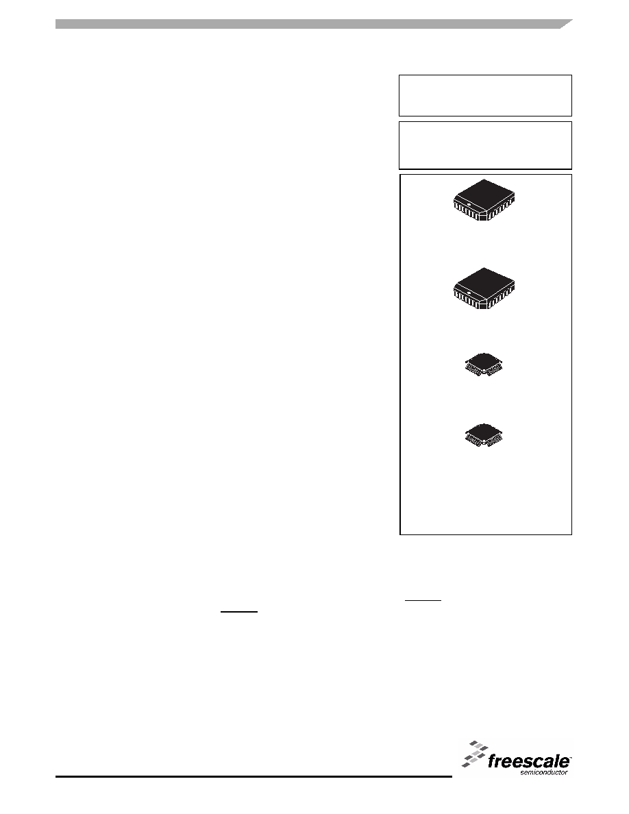
Notes:
(1) FN, FA suffix: leaded terminatons
(2) EI, AC suffix: lead-free, RoHS-compliant,
EPP
FN SUFFIX(1)
28-LEAD PLCC PACKAGE
CASE 776-02
EI SUFFIX(2)
28-LEAD PLCC PACKAGE
CASE 776-02
FA SUFFIX(1)
32-LEAD LQFP PACKAGE
CASE 873A-03
AC SUFFIX(2)
32-LEAD LQFP PACKAGE
CASE 873A-03
相关PDF资料 |
PDF描述 |
|---|---|
| MCL908QY1DT | 8-BIT, FLASH, 2 MHz, MICROCONTROLLER, PDSO16 |
| MCL908QY2PE | 8-BIT, FLASH, 2 MHz, MICROCONTROLLER, PDIP16 |
| M34509G4-XXXFP | 4-BIT, OTPROM, 6 MHz, MICROCONTROLLER, PDSO24 |
| M3823AGFFP | 8-BIT, MROM, 10 MHz, MICROCONTROLLER, PQFP80 |
| MPC8280VRMIBX | 32-BIT, 266 MHz, RISC PROCESSOR, PBGA516 |
相关代理商/技术参数 |
参数描述 |
|---|---|
| MPC92439KLF | 制造商:IDT 制造商全称:Integrated Device Technology 功能描述:900MHz, Low Voltage, LVPECL Clock Syntheesizer |
| MPC92469 | 制造商:IDT 制造商全称:Integrated Device Technology 功能描述:400 MHz Low Voltage PECL Clock Synthesizer w/Spread Spectrum |
| MPC92469AC | 功能描述:时钟合成器/抖动清除器 LVPECL Clock Synthesizer RoHS:否 制造商:Skyworks Solutions, Inc. 输出端数量: 输出电平: 最大输出频率: 输入电平: 最大输入频率:6.1 GHz 电源电压-最大:3.3 V 电源电压-最小:2.7 V 封装 / 箱体:TSSOP-28 封装:Reel |
| MPC92469ACR2 | 功能描述:IC SYNTHESIZER LVPECL 32-LQFP RoHS:是 类别:集成电路 (IC) >> 时钟/计时 - 时钟发生器,PLL,频率合成器 系列:- 标准包装:1,000 系列:- 类型:时钟/频率合成器,扇出分配 PLL:- 输入:- 输出:- 电路数:- 比率 - 输入:输出:- 差分 - 输入:输出:- 频率 - 最大:- 除法器/乘法器:- 电源电压:- 工作温度:- 安装类型:表面贴装 封装/外壳:56-VFQFN 裸露焊盘 供应商设备封装:56-VFQFP-EP(8x8) 包装:带卷 (TR) 其它名称:844S012AKI-01LFT |
| MPC9259 | 制造商:MOTOROLA 制造商全称:Motorola, Inc 功能描述:900 MHz LOW VOLTAGE LVDS CLOCK SYNTHESIZER |
发布紧急采购,3分钟左右您将得到回复。