- 您现在的位置:买卖IC网 > PDF目录69037 > MPC9299FA (MOTOROLA INC) 400 MHz, OTHER CLOCK GENERATOR, PQFP32 PDF资料下载
参数资料
| 型号: | MPC9299FA |
| 厂商: | MOTOROLA INC |
| 元件分类: | 时钟产生/分配 |
| 英文描述: | 400 MHz, OTHER CLOCK GENERATOR, PQFP32 |
| 封装: | LQFP-32 |
| 文件页数: | 6/12页 |
| 文件大小: | 184K |
| 代理商: | MPC9299FA |
MPC9229
TIMING SOLUTIONS
3
MOTOROLA
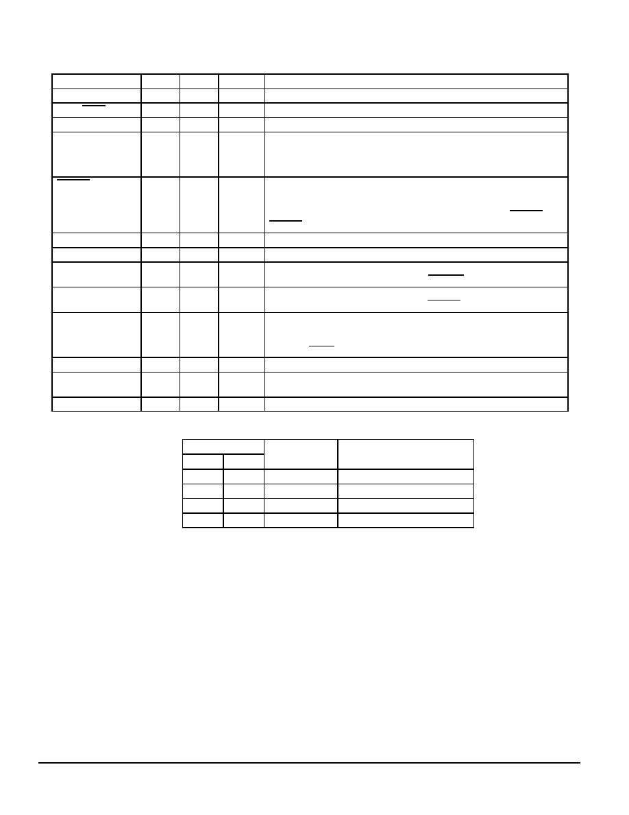
Table 1. Pin Configuration
Pin
I/O
Default
Type
Function
XTAL_IN, XTAL_OUT
Analog
Crystal oscillator interface
FOUT, FOUT
Output
LVPECL
Differential clock output
TEST
Output
LVCMOS
Test and device diagnosis output
S_LOAD
Input
0
LVCMOS
Serial configuration control input.
This inputs controls the loading of the configuration latches with the contents of
the shift register. The latches will be transparent when this signal is high, thus the
data must be stable on the high-to-low transition.
P_LOAD
Input
1
LVCMOS
Parallel configuration control input.
This input controls the loading of the configuration latches with the content of the
parallel inputs (M and N). The latches will be transparent when this signal is low,
thus the parallel data must be stable on the low-to-high transition of P_LOAD.
P_LOAD is state sensitive
S_DATA
Input
0
LVCMOS
Serial configuration data input.
S_CLOCK
Input
0
LVCMOS
Serial configuration clock input.
M[0:8]
Input
1
LVCMOS
Parallel configuration for PLL feedback divider (M).
M is sampled on the low-to-high transition of P_LOAD.
N[1:0]
Input
1
LVCMOS
Parallel configuration for Post-PLL divider (N).
N is sampled on the low-to-high transition of P_LOAD
OE
Input
1
LVCMOS
Output enable (active high)
The output enable is synchronous to the output clock to eliminate the possibility of
runt pulses on the FOUT output. OE = L low stops FOUT in the logic low state
(FOUT =L,FOUT =H)
GND
Supply
Ground
Negative power supply (GND)
VCC
Supply
VCC
Positive power supply for I/O and core. All VCC pins must be connected to the
positive power supply for correct operation
VCC_PLL
Supply
VCC
PLL positive power supply (analog power supply)
Table 2. Output frequency range and PLL Post-divider N
N
O
di i i
O
f
1
0
Output division
Output frequency range
0
1
200 - 400 MHz
0
1
2
100 - 200 MHz
1
0
4
50 - 100 MHz
1
8
25 - 50 MHz
相关PDF资料 |
PDF描述 |
|---|---|
| MPC930FA | 140 MHz, PROC SPECIFIC CLOCK GENERATOR, PQFP32 |
| MPC930FA | 140 MHz, PROC SPECIFIC CLOCK GENERATOR, PQFP32 |
| MPC972FA | 125 MHz, PROC SPECIFIC CLOCK GENERATOR, PQFP52 |
| MPC9850VF | 500 MHz, PROC SPECIFIC CLOCK GENERATOR, PBGA100 |
| MPC9850VMR2 | 500 MHz, PROC SPECIFIC CLOCK GENERATOR, PBGA100 |
相关代理商/技术参数 |
参数描述 |
|---|---|
| MPC930 | 制造商:MOTOROLA 制造商全称:Motorola, Inc 功能描述:LOW VOLTAGE PLL CLOCK DRIVER |
| MPC930A43 F44A WAF | 制造商:Motorola Inc 功能描述: |
| MPC931 | 制造商:Motorola Inc 功能描述: |
| MPC9315 | 制造商:MOTOROLA 制造商全称:Motorola, Inc 功能描述:2.5V and 3.3V CMOS PLL Clock Generator and Driver |
| MPC9315AC | 功能描述:锁相环 - PLL 2.5 3.3V 160MHz Clock Generator RoHS:否 制造商:Silicon Labs 类型:PLL Clock Multiplier 电路数量:1 最大输入频率:710 MHz 最小输入频率:0.002 MHz 输出频率范围:0.002 MHz to 808 MHz 电源电压-最大:3.63 V 电源电压-最小:1.71 V 最大工作温度:+ 85 C 最小工作温度:- 40 C 封装 / 箱体:QFN-36 封装:Tray |
发布紧急采购,3分钟左右您将得到回复。