- 您现在的位置:买卖IC网 > PDF目录132964 > MPC9299FN (MOTOROLA INC) 400 MHz, OTHER CLOCK GENERATOR, PQCC28 PDF资料下载
参数资料
| 型号: | MPC9299FN |
| 厂商: | MOTOROLA INC |
| 元件分类: | 时钟产生/分配 |
| 英文描述: | 400 MHz, OTHER CLOCK GENERATOR, PQCC28 |
| 封装: | PLASTIC, LCC-28 |
| 文件页数: | 11/12页 |
| 文件大小: | 184K |
| 代理商: | MPC9299FN |
MPC9229
MOTOROLA
TIMING SOLUTIONS
8
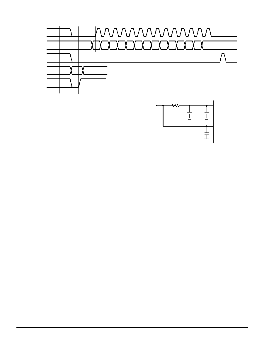
Figure 4. Serial Interface Timing Diagram
S_CLOCK
S_DATA
S_LOAD
M[8:0]
N[1:0]
P_LOAD
T2
T1
T0
N1
N0
M8
M7
M6
M5
M4
M3
M2
M1
M0
M, N
First
Bit
Last
Bit
Power Supply Filtering
The MPC9229 is a mixed analog/digital product. Its analog
circuitry is naturally susceptible to random noise, especially if
this noise is seen on the power supply pins. Random noise on
the VCC_PLL pin impacts the device characteristics. The
MPC9229 provides separate power supplies for the digital
circuitry (VCC) and the internal PLL (VCC_PLL) of the device.
The purpose of this design technique is to try and isolate the
high switching noise digital outputs from the relatively
sensitive internal analog phase–locked loop. In a controlled
environment such as an evaluation board, this level of
isolation is sufficient. However, in a digital system environment
where it is more difficult to minimize noise on the power
supplies a second level of isolation may be required. The
simplest form of isolation is a power supply filter on the
VCC_PLL pin for the MPC9229. Figure 5 illustrates a typical
power supply filter scheme. The MPC9229 is most susceptible
to noise with spectral content in the 1 kHz to 1 MHz range.
Therefore, the filter should be designed to target this range.
The key parameter that needs to be met in the final filter design
is the DC voltage drop that will be seen between the VCC
supply and the MPC9229 pin of the MPC9229. From the data
sheet, the VCC_PLL current (the current sourced through the
VCC_PLL pin) is maximum 20 mA, assuming that a minimum
of 2.835 V must be maintained on the VCC_PLL pin. The
resistor shown in Figure 5 must have a resistance of 10-15
to meet the voltage drop criteria. The RC filter pictured will
provide a broadband filter with approximately 100:1
attenuation for noise whose spectral content is above 20 kHz.
As the noise frequency crosses the series resonant point of an
individual capacitor its overall impedance begins to look
inductive and thus increases with increasing frequency. The
parallel capacitor combination shown ensures that a low
impedance path to ground exists for frequencies well above
the bandwidth of the PLL. Generally, the resistor/capacitor
filter will be cheaper, easier to implement and provide an
adequate level of supply filtering. A higher level of attenuation
can be achieved by replacing the resistor with an appropriate
valued inductor. A 1000 H choke will show a significant
impedance at 10 kHz frequencies and above. Because of the
current draw and the voltage that must be maintained on the
VCC_PLL pin, a low DC resistance inductor is required (less
than 15 ).
Figure 5. VCC PLL Power Supply Filter
VCC_PLL
VCC
MPC9229
C1,C2 = 0.01...0.1 F
VCC
CF =22 F
RF =10--15
C2
C1
Layout Recommendations
The MPC9229 provides sub–nanosecond output edge
rates and thus a good power supply bypassing scheme is a
must. Figure 6 shows a representative board layout for the
MPC9229. There exists many different potential board layouts
and the one pictured is but one. The important aspect of the
layout in Figure 6 is the low impedance connections between
VCC and GND for the bypass capacitors. Combining good
quality general purpose chip capacitors with good PCB layout
techniques will produce effective capacitor resonances at
frequencies adequate to supply the instantaneous switching
current for the MPC9229 outputs. It is imperative that low
inductance chip capacitors are used; it is equally important
that the board layout does not introduce back all of the
inductance saved by using the leadless capacitors. Thin
interconnect traces between the capacitor and the power
plane should be avoided and multiple large vias should be
used to tie the capacitors to the buried power planes. Fat
interconnect and large vias will help to minimize layout
induced inductance and thus maximize the series resonant
point of the bypass capacitors. Note the dotted lines circling
the crystal oscillator connection to the device. The oscillator is
a series resonant circuit and the voltage amplitude across the
crystal is relatively small. It is imperative that no actively
switching signals cross under the crystal as crosstalk energy
coupled to these lines could significantly impact the jitter of the
device. Special attention should be paid to the layout of the
crystal to ensure a stable, jitter free interface between the
crystal and the on–board oscillator. Although the MPC9229
has several design features to minimize the susceptibility to
相关PDF资料 |
PDF描述 |
|---|---|
| M48T512Y-85PM1 | REAL TIME CLOCK, PDIP32 |
| MB89202YPFV | 8-BIT, MROM, 12.5 MHz, MICROCONTROLLER, PDSO34 |
| MPC7410THX450LE | 32-BIT, 450 MHz, RISC PROCESSOR, CBGA360 |
| M48T08Y-10MH1F | 0 TIMER(S), REAL TIME CLOCK, PDSO28 |
| MK2703SILFTR | 27 MHz, OTHER CLOCK GENERATOR, PDSO8 |
相关代理商/技术参数 |
参数描述 |
|---|---|
| MPC930 | 制造商:MOTOROLA 制造商全称:Motorola, Inc 功能描述:LOW VOLTAGE PLL CLOCK DRIVER |
| MPC930A43 F44A WAF | 制造商:Motorola Inc 功能描述: |
| MPC931 | 制造商:Motorola Inc 功能描述: |
| MPC9315 | 制造商:MOTOROLA 制造商全称:Motorola, Inc 功能描述:2.5V and 3.3V CMOS PLL Clock Generator and Driver |
| MPC9315AC | 功能描述:锁相环 - PLL 2.5 3.3V 160MHz Clock Generator RoHS:否 制造商:Silicon Labs 类型:PLL Clock Multiplier 电路数量:1 最大输入频率:710 MHz 最小输入频率:0.002 MHz 输出频率范围:0.002 MHz to 808 MHz 电源电压-最大:3.63 V 电源电压-最小:1.71 V 最大工作温度:+ 85 C 最小工作温度:- 40 C 封装 / 箱体:QFN-36 封装:Tray |
发布紧急采购,3分钟左右您将得到回复。