- 您现在的位置:买卖IC网 > PDF目录69037 > MPC930FA (FREESCALE SEMICONDUCTOR INC) 140 MHz, PROC SPECIFIC CLOCK GENERATOR, PQFP32 PDF资料下载
参数资料
| 型号: | MPC930FA |
| 厂商: | FREESCALE SEMICONDUCTOR INC |
| 元件分类: | 时钟产生/分配 |
| 英文描述: | 140 MHz, PROC SPECIFIC CLOCK GENERATOR, PQFP32 |
| 封装: | TQFP-32 |
| 文件页数: | 12/12页 |
| 文件大小: | 326K |
| 代理商: | MPC930FA |
MPC930 MPC931
MOTOROLA ADVANCED CLOCK DRIVERS DEVICE DATA
57
outputs are switching at the same frequency there is no edge
dis p lac e ment and the jitter is reduc ed to that of
the PLL.
Figure 12 graphically represents the PLL jitter of the
MPC930/931. The data was taken for several different output
configurations. Because of the relatively few outputs on the
MPC930/931, the multimodal distribution is of a second order
affect on the 930/931 and can be ignored. As one can see in
the figure the PLL jitter is much less dependent on output con-
figuration than on internal VCO frequency. However, for a giv-
en VCO frequency, a lower output frequency produces more
jitter.
Figure 12. RMS Jitter versus VCO Frequency
(Qa0 Output)
10
15
20
25
30
35
40
45
80
120
160
200
240
280
Conf 1
Conf 2
Conf 1 = Qa=÷2, Qb=Qc=÷4
Conf 2 = Qa=÷2, Qb=Qc=Shut Down
Conf 3 = Qa=÷4, Qb=Qc=Shut Down
VCO Frequency (MHz)
RMS
Jitter
(ps)
Figure 13. RMS Jitter versus Output Frequency
(Qa0 Output)
10
15
20
25
30
35
20
40
60
80
100
120
140
Frequency Output (MHz)
RMS
Jitter
(ps)
Conf 2 = Qa=÷2, Qb=Qc=Shut Down
Conf 3 = Qa=÷4, Qb=Qc=Shut Down
Conf 3
Conf 2
Conf 3
Finally from the data there are some general guidelines that,
if followed, will minimize the output jitter of the device. First and
foremost always configure the device such that the VCO runs
as fast as possible. This is by far the most critical parameter in
minimizing jitter. Second keep the reference frequency as high
as possible. More frequent updates at the phase detector will
help to reduce jitter. Note that if there is a tradeoff between
higher reference frequencies and higher VCO frequency al-
ways chose the higher VCO frequency to minimize jitter. The
third guideline is to try to shut down outputs that are unused.
Minimizing the number of switching outputs will minimize out-
put jitter.
Power Supply Filtering
The MPC930/931 is a mixed analog/digital product and as
such it exhibits some sensitivities that would not necessarily be
seen on a fully digital product. Analog circuitry is naturally sus-
ceptible to random noise, especially if this noise is seen on the
power supply pins. The MPC930/931 provides separate power
supplies for the output buffers (VCCO) and the internal PLL
(PLL_VCC) of the device. The purpose of this design tech-
nique is to try and isolate the high switching noise digital out-
puts from the relatively sensitive internal analog phase–locked
loop. In a controlled environment such as an evaluation board
this level of isolation is sufficient. However, in a digital system
environment where it is more difficult to minimize noise on the
power supplies a second level of isolation may be required.
The simplest form of isolation is a power supply filter on the
PLL_VCC pin for the MPC930/931.
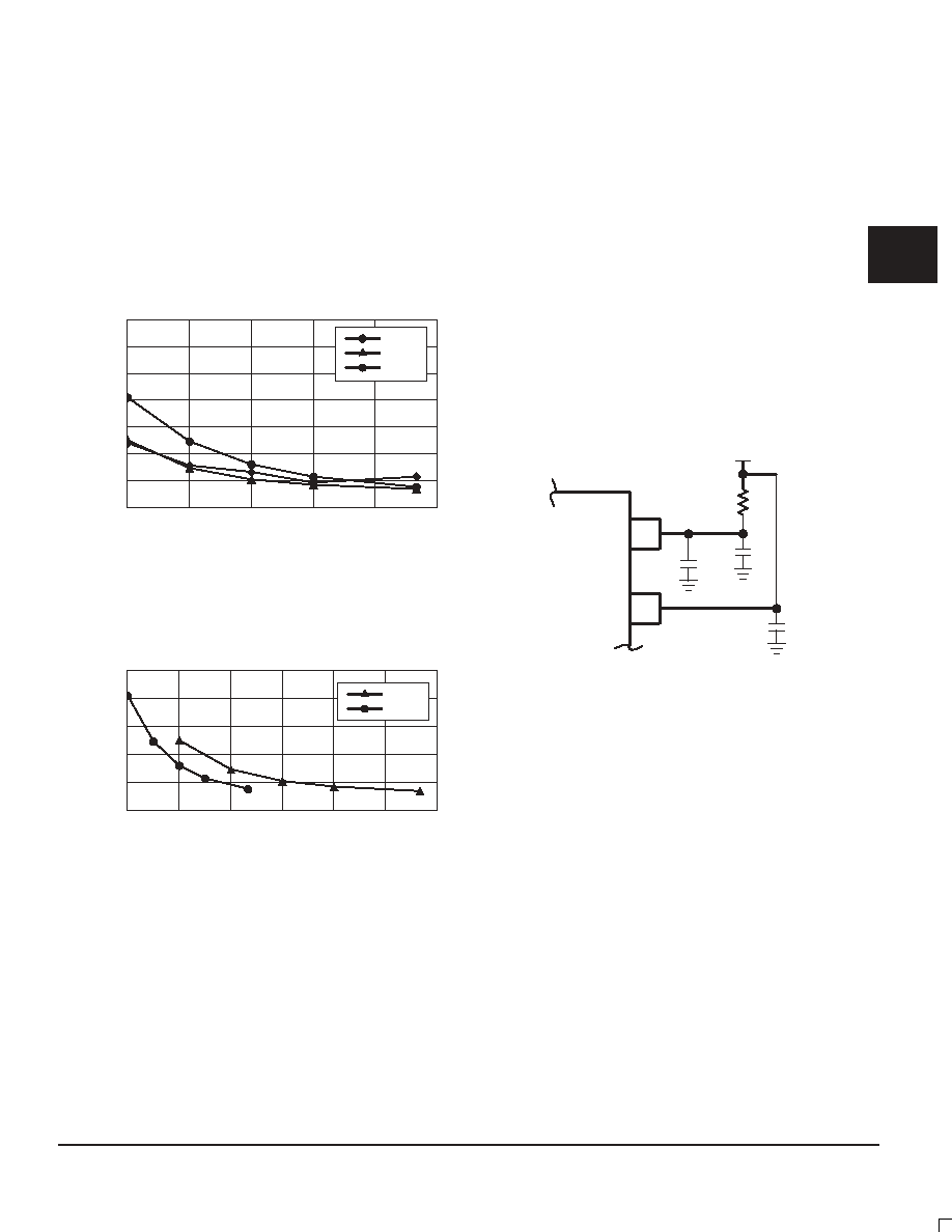
Figure 14. Power Supply Filter
PLL_VCC
VCC
MPC930/931
0.01F
22F
0.01F
3.3V
RS=10-15
Figure 14 illustrates a typical power supply filter scheme.
The MPC930/931 is most susceptible to noise with spectral
content in the 1KHz to 1MHz range. Therefore the filter should
be designed to target this range. The key parameter that needs
to be met in the final filter design is the DC voltage drop that will
be seen between the VCC supply and the PLL_VCC pin of the
MPC930/931. From the data sheet the IPLL_VCC current (the
current sourced through the PLL_VCC pin) is typically 15mA
(20mA maximum), assuming that a minimum of 3.0V must be
maintained on the PLL_VCC pin very little DC voltage drop can
be tolerated when a 3.3V VCC supply is used. The resistor
shown in Figure 14 must have a resistance of 10–15
to meet
the voltage drop criteria. The RC filter pictured will provide a
broadband filter with approximately 100:1 attenuation for noise
whose spectral content is above 20KHz. As the noise frequen-
cy crosses the series resonant point of an individual capacitor
it’s overall impedance begins to look inductive and thus in-
creases with increasing frequency. The parallel capacitor com-
bination shown ensures that a low impedance path to ground
exists for frequencies well above the bandwidth of the PLL.
Although the MPC930/931 has several design features to
minimize the susceptibility to power supply noise (isolated
power and grounds and fully differential PLL) there still may be
applications in which overall performance is being degraded
due to system power supply noise. The power supply filter
2
F
re
e
sc
a
le
S
e
m
ic
o
n
d
u
c
to
r,
I
Freescale Semiconductor, Inc.
For More Information On This Product,
Go to: www.freescale.com
n
c
..
.
相关PDF资料 |
PDF描述 |
|---|---|
| MPC972FA | 125 MHz, PROC SPECIFIC CLOCK GENERATOR, PQFP52 |
| MPC9850VF | 500 MHz, PROC SPECIFIC CLOCK GENERATOR, PBGA100 |
| MPC9850VMR2 | 500 MHz, PROC SPECIFIC CLOCK GENERATOR, PBGA100 |
| MPC9850VMR2 | 500 MHz, PROC SPECIFIC CLOCK GENERATOR, PBGA100 |
| MPC9850VFR2 | 500 MHz, PROC SPECIFIC CLOCK GENERATOR, PBGA100 |
相关代理商/技术参数 |
参数描述 |
|---|---|
| MPC931 | 制造商:Motorola Inc 功能描述: |
| MPC9315 | 制造商:MOTOROLA 制造商全称:Motorola, Inc 功能描述:2.5V and 3.3V CMOS PLL Clock Generator and Driver |
| MPC9315AC | 功能描述:锁相环 - PLL 2.5 3.3V 160MHz Clock Generator RoHS:否 制造商:Silicon Labs 类型:PLL Clock Multiplier 电路数量:1 最大输入频率:710 MHz 最小输入频率:0.002 MHz 输出频率范围:0.002 MHz to 808 MHz 电源电压-最大:3.63 V 电源电压-最小:1.71 V 最大工作温度:+ 85 C 最小工作温度:- 40 C 封装 / 箱体:QFN-36 封装:Tray |
| MPC9315ACR2 | 功能描述:时钟发生器及支持产品 FSL 1-8 LVCMOS PLL Clock Generator RoHS:否 制造商:Silicon Labs 类型:Clock Generators 最大输入频率:14.318 MHz 最大输出频率:166 MHz 输出端数量:16 占空比 - 最大:55 % 工作电源电压:3.3 V 工作电源电流:1 mA 最大工作温度:+ 85 C 安装风格:SMD/SMT 封装 / 箱体:QFN-56 |
| MPC9315FA | 功能描述:锁相环 - PLL 2.5 3.3V 160MHz Clock Generator RoHS:否 制造商:Silicon Labs 类型:PLL Clock Multiplier 电路数量:1 最大输入频率:710 MHz 最小输入频率:0.002 MHz 输出频率范围:0.002 MHz to 808 MHz 电源电压-最大:3.63 V 电源电压-最小:1.71 V 最大工作温度:+ 85 C 最小工作温度:- 40 C 封装 / 箱体:QFN-36 封装:Tray |
发布紧急采购,3分钟左右您将得到回复。