- 您现在的位置:买卖IC网 > PDF目录29137 > MPC9443AE (FREESCALE SEMICONDUCTOR INC) 9443 SERIES, LOW SKEW CLOCK DRIVER, 16 TRUE OUTPUT(S), 0 INVERTED OUTPUT(S), PQFP48 PDF资料下载
参数资料
| 型号: | MPC9443AE |
| 厂商: | FREESCALE SEMICONDUCTOR INC |
| 元件分类: | 时钟及定时 |
| 英文描述: | 9443 SERIES, LOW SKEW CLOCK DRIVER, 16 TRUE OUTPUT(S), 0 INVERTED OUTPUT(S), PQFP48 |
| 封装: | 7 X 7 MM, PLASTIC, LQFP-48 |
| 文件页数: | 10/12页 |
| 文件大小: | 209K |
| 代理商: | MPC9443AE |
MPC9443
598
FREESCALE SEMICONDUCTOR ADVANCED CLOCK DRIVERS DEVICE DATA
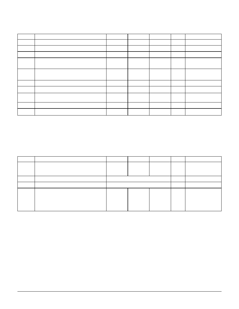
Table 11. DC Characteristics (VCC = 3.3 V ± 5%, any VCCA,B,C,D = 2.5 V ± 5% or 3.3 V ± 5% (mixed), TA = –40 to +85°C)
Symbol
Characteristics
Min
Typ
Max
Unit
Condition
VIH
Input High Voltage
2.0
VCC + 0.3
V
LVCMOS
VIL
Input Low Voltage
–0.3
0.8
V
LVCMOS
IIN
Input Current1
1.
Input pull-up / pull-down resistors influence input current.
200
A
VOH
Output High Voltage
2.5 V output
3.3 V output
1.7
2.0
V
IOH = –15 mA
2
IOH = 24 mA
2
2.
The MPC9443 is capable of driving 50
transmission lines on the incident edge. Each output drives one 50 parallel terminated transmission
line to a termination voltage of VTT. Alternatively, the device drives up to two 50 series terminated transmission lines (for VCC = 3.3 V) or one
50
series terminated transmission line (for V
CC =2.5 V).
VOL
Output Low Voltage
2.5 V output
3.3 V output
0.6
0.55
V
IOL = 15 mA
2
IOL = 24 mA
2
VPP
Peak-to-Peak Input Voltage
PCLK0,1
250
mV
LVPECL
VCMR
3
3.
VCMR (DC) is the crosspoint of the differential input signal. Functional operation is obtained when the crosspoint is within the VCMR range and the
input swing lies within the VPP (DC) specification.
Common Mode Range
PCLK0, 1
1.1
VCC – 0.6
V
LVPECL
ZOUT
Output Impedance
2.5 V output
3.3 V output
22
19
CPD
Power Dissipation Capacitance
10
pF
Per Output
ICCQ
4
4.
ICCQ is the DC current consumption of the device with all outputs open and the input in its default state or open.
Maximum Quiescent Supply Current
3.0
mA
All VCC Pins
Table 12. AC Characteristics (VCC = 3.3 V ± 5%, any VCCA,B,C,D = 2.5 V ± 5% or 3.3 V ± 5% (mixed), TA = –40 to +85°C)
1 2
1.
AC characteristics apply for parallel output termination of 50
to V
TT.
2.
This table only specifies AC parameter in mixed voltage supply conditions that vary from the corresponding AC tables. For all other parameters,
see Table 8 (for 3.3 V outputs) or Table 10 (for 2.5 V outputs)
Symbol
Characteristics
Min
Typ
Max
Unit
Condition
tsk(LH, HL) Output-to-Output Skew3
Any output, same output divider
Any output, any output divider
3.
tsk(LH, HL) includes both device skew referenced to the rising output edge and device skew referenced to the falling output edge.
275
350
ps
tsk(PP)
Device-to-Device Skew
See Table 8 (3.3 V AC Characteristics)
tPLH, HL
Propagation Delay
See Table 8 (3.3 V AC Characteristics)
tSK(P)
DCQ
Output Pulse Skew4
Using PCLK0,1
Using CCLK
Output Duty Cycle
fQ<140 MHz and using CCLK
fQ<250 MHz and using PCLK0,1
4.
Output pulse skew is the absolute difference of the propagation delay times: | tPLH – tPHL |
45
50
400
500
55
ps
%
DCREF = 50%
相关PDF资料 |
PDF描述 |
|---|---|
| MPC9446FAR2 | 9446 SERIES, LOW SKEW CLOCK DRIVER, 10 TRUE OUTPUT(S), 0 INVERTED OUTPUT(S), PQFP32 |
| MPC9446FAR2 | 9446 SERIES, LOW SKEW CLOCK DRIVER, 10 TRUE OUTPUT(S), 0 INVERTED OUTPUT(S), PQFP32 |
| MPC952FAR2 | LVCMOS/LVTTL SERIES, PLL BASED CLOCK DRIVER, 11 TRUE OUTPUT(S), 0 INVERTED OUTPUT(S), PQFP32 |
| MPC952FA | 952 SERIES, PLL BASED CLOCK DRIVER, 11 TRUE OUTPUT(S), 0 INVERTED OUTPUT(S), PQFP32 |
| MPC954DT | MPC900 SERIES, PLL BASED CLOCK DRIVER, 10 TRUE OUTPUT(S), 0 INVERTED OUTPUT(S), PDSO24 |
相关代理商/技术参数 |
参数描述 |
|---|---|
| MPC9443AER2 | 功能描述:时钟驱动器及分配 FSL 1-16 LVCMOS Fanout Buffer RoHS:否 制造商:Micrel 乘法/除法因子:1:4 输出类型:Differential 最大输出频率:4.2 GHz 电源电压-最大: 电源电压-最小:5 V 最大工作温度:+ 85 C 封装 / 箱体:SOIC-8 封装:Reel |
| MPC9443FA | 功能描述:时钟缓冲器 2.5 3.3V 250MHz Clock Generator RoHS:否 制造商:Texas Instruments 输出端数量:5 最大输入频率:40 MHz 传播延迟(最大值): 电源电压-最大:3.45 V 电源电压-最小:2.375 V 最大功率耗散: 最大工作温度:+ 85 C 最小工作温度:- 40 C 封装 / 箱体:LLP-24 封装:Reel |
| MPC9443FAR2 | 功能描述:时钟驱动器及分配 FSL 1-16 LVCMOS Fanout Buffer RoHS:否 制造商:Micrel 乘法/除法因子:1:4 输出类型:Differential 最大输出频率:4.2 GHz 电源电压-最大: 电源电压-最小:5 V 最大工作温度:+ 85 C 封装 / 箱体:SOIC-8 封装:Reel |
| MPC9446 | 制造商:MOTOROLA 制造商全称:Motorola, Inc 功能描述:2.5V and 3.3V LVCMOS Clock Fanout Buffer |
| MPC9446AC | 功能描述:时钟缓冲器 2.5 3.3V 275MHz Clock Generator RoHS:否 制造商:Texas Instruments 输出端数量:5 最大输入频率:40 MHz 传播延迟(最大值): 电源电压-最大:3.45 V 电源电压-最小:2.375 V 最大功率耗散: 最大工作温度:+ 85 C 最小工作温度:- 40 C 封装 / 箱体:LLP-24 封装:Reel |
发布紧急采购,3分钟左右您将得到回复。