- 您现在的位置:买卖IC网 > PDF目录8752 > MPC9443AE (IDT, Integrated Device Technology Inc)IC CLK BUFF DVDR MUX 3:16 48LQFP PDF资料下载
参数资料
| 型号: | MPC9443AE |
| 厂商: | IDT, Integrated Device Technology Inc |
| 文件页数: | 9/15页 |
| 文件大小: | 0K |
| 描述: | IC CLK BUFF DVDR MUX 3:16 48LQFP |
| 标准包装: | 250 |
| 类型: | 扇出缓冲器(分配),除法器,多路复用器 |
| 电路数: | 1 |
| 比率 - 输入:输出: | 3:16 |
| 差分 - 输入:输出: | 是/无 |
| 输入: | LVCMOS,LVPECL |
| 输出: | LVCMOS |
| 频率 - 最大: | 350MHz |
| 电源电压: | 2.375 V ~ 3.465 V |
| 工作温度: | -40°C ~ 85°C |
| 安装类型: | 表面贴装 |
| 封装/外壳: | 48-LQFP |
| 供应商设备封装: | 48-TQFP(7x7) |
| 包装: | 托盘 |
| 其它名称: | 800-2221 MPC9443AEIDT-ND |
MPC9443 REVISION 6 AUGUST 23, 2013
3
2013 Integrated Device Technology, Inc.
MPC9443 Data Sheet
2.5V, 3.3V LVCMOS CLOCK FANOUT BUFFER
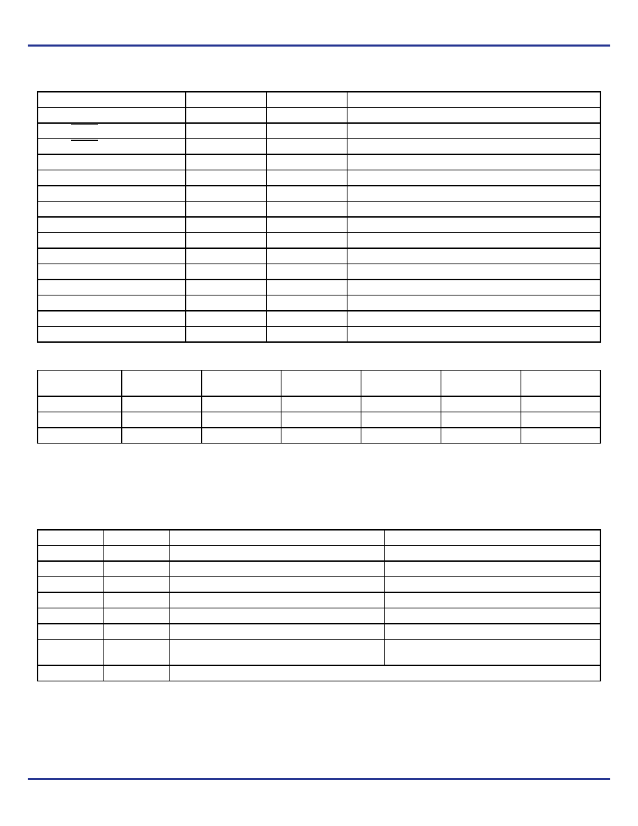
Table 1. Pin Configuration
Pin
I/O
Type
Function
CCLK
Input
LVCMOS
LVCMOS clock inputs
PCLK0, PCLK0
Input
LVCMOS
LVPECL differential clock input
PCLK1, PCLK1
Input
LVCMOS
LVPECL differential clock input
FSELA, FSELB, FSELC, FSELD
Input
LVCMOS
Output bank divide select input
CCLK_SEL
Input
LVCMOS
LVCMOS/LVPECL clock input select
PCLK_SEL
Input
LVCMOS
PCLK0/PCLK1 clock input select
OE0, OE1
Input
LVCMOS
Output tristate control
CLK_STOP
Input
LVCMOS
Synchronous output enable/disable (clock stop) control
GND
Supply
Negative voltage supply
VCCA, VCCB, VCCC, VCCD
Supply
Positive voltage supply output bank (VCC)
VCC
Supply
Positive voltage supply core (VCC)
QA0 to QA4
Output
LVCMOS
Bank A outputs
QB0 to QB2
Output
LVCMOS
Bank B outputs
QC0 to QC2
Output
LVCMOS
Bank C outputs
QD0 to QD4
Output
LVCMOS
Bank D outputs
Table 2. Supported Single and Dual Supply Configurations
Supply Voltage
Configuration
VCC(1)
1. VCC is the positive power supply of the device core and input circuitry. VCC voltage defines the input threshold and levels.
VCCA(2)
2. VCCA is the positive power supply of the bank A outputs. VCCA voltage defines bank A output levels.
VCCB(3)
3. VCCB is the positive power supply of the bank B outputs. VCCB voltage defines bank B output levels.
VCCC(4)
4. VCCC is the positive power supply of the bank C outputs. VCCC voltage defines bank C output levels.
VCCD(5)
5. VCCD is the positive power supply of the bank D outputs. VCCD voltage defines bank D output levels.
GND
3.3 V Supply
3.3 V
0 V
Mixed Mode Supply
3.3 V
3.3 V or 2.5 V
0 V
2.5 V Supply
2.5 V
0 V
Table 3. . Function Table (Controls)
Control
Default
0
1
CCLK_SEL
0
PCLK or PCLK1 active (LVPECL clock mode)
CCLK active (LVCMOS clock mode)
PCLK_SEL
0
PCLK0 active, PCLK1 inactive
PCLK1 active, PCLK0 inactive
FSELA
0
fQA0:4 = fREF
fQA0:4 = fREF 2
FSELB
0
fQB0:2 = fREF
fQB0:2 = fREF 2
FSELC
0
fQC0:2 = fREF
fQC0:2 = fREF 2
FSELD
0
fQD0:4 = fREF
fQD0:4 = fREF 2
CLK_STOP
0
Normal operation
Outputs are synchronously disabled (stopped) in logic low
state
OE0, OE1
00
Asynchronous output enable control. See Table 4.
相关PDF资料 |
PDF描述 |
|---|---|
| VE-24X-MW-F1 | CONVERTER MOD DC/DC 5.2V 100W |
| VE-BNP-IU-B1 | CONVERTER MOD DC/DC 13.8V 200W |
| VE-24W-MW-F4 | CONVERTER MOD DC/DC 5.5V 100W |
| VE-24W-MW-F3 | CONVERTER MOD DC/DC 5.5V 100W |
| VE-24W-MW-F2 | CONVERTER MOD DC/DC 5.5V 100W |
相关代理商/技术参数 |
参数描述 |
|---|---|
| MPC9443AER2 | 功能描述:时钟驱动器及分配 FSL 1-16 LVCMOS Fanout Buffer RoHS:否 制造商:Micrel 乘法/除法因子:1:4 输出类型:Differential 最大输出频率:4.2 GHz 电源电压-最大: 电源电压-最小:5 V 最大工作温度:+ 85 C 封装 / 箱体:SOIC-8 封装:Reel |
| MPC9443FA | 功能描述:时钟缓冲器 2.5 3.3V 250MHz Clock Generator RoHS:否 制造商:Texas Instruments 输出端数量:5 最大输入频率:40 MHz 传播延迟(最大值): 电源电压-最大:3.45 V 电源电压-最小:2.375 V 最大功率耗散: 最大工作温度:+ 85 C 最小工作温度:- 40 C 封装 / 箱体:LLP-24 封装:Reel |
| MPC9443FAR2 | 功能描述:时钟驱动器及分配 FSL 1-16 LVCMOS Fanout Buffer RoHS:否 制造商:Micrel 乘法/除法因子:1:4 输出类型:Differential 最大输出频率:4.2 GHz 电源电压-最大: 电源电压-最小:5 V 最大工作温度:+ 85 C 封装 / 箱体:SOIC-8 封装:Reel |
| MPC9446 | 制造商:MOTOROLA 制造商全称:Motorola, Inc 功能描述:2.5V and 3.3V LVCMOS Clock Fanout Buffer |
| MPC9446AC | 功能描述:时钟缓冲器 2.5 3.3V 275MHz Clock Generator RoHS:否 制造商:Texas Instruments 输出端数量:5 最大输入频率:40 MHz 传播延迟(最大值): 电源电压-最大:3.45 V 电源电压-最小:2.375 V 最大功率耗散: 最大工作温度:+ 85 C 最小工作温度:- 40 C 封装 / 箱体:LLP-24 封装:Reel |
发布紧急采购,3分钟左右您将得到回复。