- 您现在的位置:买卖IC网 > PDF目录29137 > MPC9446FAR2 (INTEGRATED DEVICE TECHNOLOGY INC) 9446 SERIES, LOW SKEW CLOCK DRIVER, 10 TRUE OUTPUT(S), 0 INVERTED OUTPUT(S), PQFP32 PDF资料下载
参数资料
| 型号: | MPC9446FAR2 |
| 厂商: | INTEGRATED DEVICE TECHNOLOGY INC |
| 元件分类: | 时钟及定时 |
| 英文描述: | 9446 SERIES, LOW SKEW CLOCK DRIVER, 10 TRUE OUTPUT(S), 0 INVERTED OUTPUT(S), PQFP32 |
| 封装: | 7 X 7 MM, PLASTIC, LQFP-32 |
| 文件页数: | 4/7页 |
| 文件大小: | 298K |
| 代理商: | MPC9446FAR2 |
6
MPC9446
MOTOROLA ADVANCED CLOCK DRIVERS DEVICE DATA
570
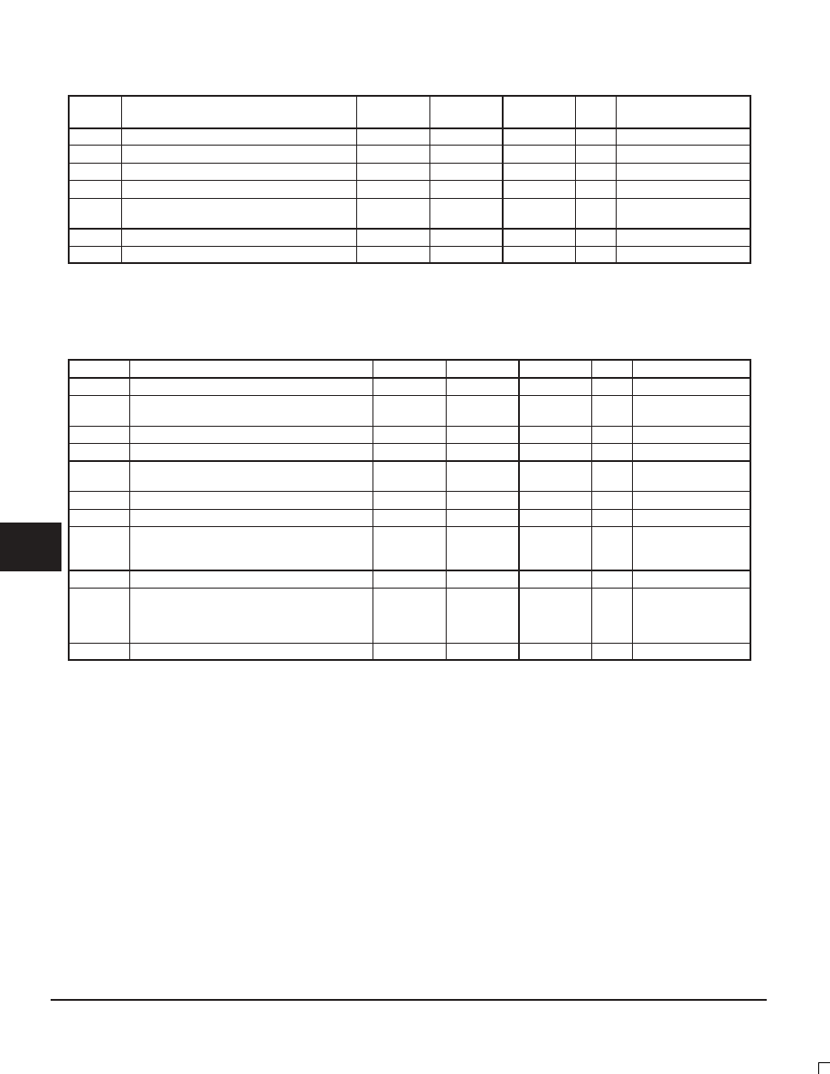
Table 6: DC CHARACTERISTICS (VCC = VCCA = VCCB = VCCC = 3.3V ±5%, TA = –40°C to +85°C)
Sym-
bol
Characteristics
Min
Typ
Max
Unit
Condition
VIH
Input High Voltage
2.0
VCC + 0.3
V
LVCMOS
VIL
Input Low Voltage
-0.3
0.8
V
LVCMOS
IIN
Input Currenta
200
A
VIN=GND or VIN=VCC
VOH
Output High Voltage
2.4
V
IOH=-24 mAb
VOL
Output Low Voltage
0.55
0.30
V
IOL= 24mAb
IOL= 12mA
ZOUT
Output Impedance
14 - 17
W
ICCQc
Maximum Quiescent Supply Current
2.0
mA
All VCC Pins
a. Input pull-up / pull-down resistors influence input current.
b. The MPC9446 is capable of driving 50
transmission lines on the incident edge. Each output drives one 50 parallel terminated transmis-
sion line to a termination voltage of VTT. Alternatively, the device drives up to two 50 series terminated transmission lines.
c. ICCQ is the DC current consumption of the device with all outputs open and the input in its default state or open.
Table 7: AC CHARACTERISTICS (VCC = VCCA = VCCB = VCCC = 3.3V ±5%, TA = –40°C to +85°C)a
Symbol
Characteristics
Min
Typ
Max
Unit
Condition
fref
Input Frequency
0
250b
MHz
fMAX
Maximum Output Frequency
÷1 output
÷2 output
0
250b
125
MHz
FSELx=0
FSELx=1
tP, REF
Reference Input Pulse Width
1.4
ns
tr, tf
CCLK Input Rise/Fall Time
1.0c
ns
0.8 to 2.0V
tPLH
tPHL
Propagation delay
CCLK0,1 to any Q
2.2
2.8
4.45
4.2
ns
tPLZ, HZ
Output Disable Time
10
ns
tPZL, LZ
Output Enable Time
10
ns
tsk(O)
Output-to-output Skew
Within one bank
Any output bank, same output divider
Any output, Any output divider
150
200
350
ps
tsk(PP)
Device-to-device Skew
2.25
ns
tSK(P)
DCQ
Output pulse skewd
Output Duty Cycle
÷1 output
÷2 output
47
45
50
200
53
55
ps
%
DCREF = 50%
DCREF = 25%-75%
tr, tf
Output Rise/Fall Time
0.1
1.0
ns
0.55 to 2.4V
a. AC characteristics apply for parallal output termination of 50
to VTT.
b. The MPC9446 is functional up to an input and output clock frequency of 350 MHz and is characterized up to 250 MHz.
c. Violation of the 1.0 ns maximum input rise and fall time limit will affect the device propagation delay, device-to-device skew, reference input
pulse width, output duty cycle and maximum frequency specifications.
d. Output pulse skew is the absolute difference of the propagation delay times: | tpLH - tpHL |.
F
re
e
sc
a
le
S
e
m
ic
o
n
d
u
c
to
r,
I
Freescale Semiconductor, Inc.
For More Information On This Product,
Go to: www.freescale.com
n
c
..
.
相关PDF资料 |
PDF描述 |
|---|---|
| MPC9446FAR2 | 9446 SERIES, LOW SKEW CLOCK DRIVER, 10 TRUE OUTPUT(S), 0 INVERTED OUTPUT(S), PQFP32 |
| MPC952FAR2 | LVCMOS/LVTTL SERIES, PLL BASED CLOCK DRIVER, 11 TRUE OUTPUT(S), 0 INVERTED OUTPUT(S), PQFP32 |
| MPC952FA | 952 SERIES, PLL BASED CLOCK DRIVER, 11 TRUE OUTPUT(S), 0 INVERTED OUTPUT(S), PQFP32 |
| MPC954DT | MPC900 SERIES, PLL BASED CLOCK DRIVER, 10 TRUE OUTPUT(S), 0 INVERTED OUTPUT(S), PDSO24 |
| MPC961PFA | 961 SERIES, PLL BASED CLOCK DRIVER, 17 TRUE OUTPUT(S), 0 INVERTED OUTPUT(S), PQFP32 |
相关代理商/技术参数 |
参数描述 |
|---|---|
| MPC9447 | 制造商:IDT 制造商全称:Integrated Device Technology 功能描述:3.3V/2.5V 1:9 LVCMOS Clock Fanout Buffer |
| MPC9447AC | 功能描述:时钟缓冲器 2.5 3.3V 250MHz Clock Generator RoHS:否 制造商:Texas Instruments 输出端数量:5 最大输入频率:40 MHz 传播延迟(最大值): 电源电压-最大:3.45 V 电源电压-最小:2.375 V 最大功率耗散: 最大工作温度:+ 85 C 最小工作温度:- 40 C 封装 / 箱体:LLP-24 封装:Reel |
| MPC9447ACR2 | 功能描述:时钟缓冲器 FSL 1-9 LVCMOS Fanout Buffer RoHS:否 制造商:Texas Instruments 输出端数量:5 最大输入频率:40 MHz 传播延迟(最大值): 电源电压-最大:3.45 V 电源电压-最小:2.375 V 最大功率耗散: 最大工作温度:+ 85 C 最小工作温度:- 40 C 封装 / 箱体:LLP-24 封装:Reel |
| MPC9447D | 制造商:MOTOROLA 制造商全称:Motorola, Inc 功能描述:3.3V/2.5V 1:9 LVCMOS Clock Fanout Buffer |
| MPC9447FA | 功能描述:时钟缓冲器 2.5 3.3V 275MHz Clock Generator RoHS:否 制造商:Texas Instruments 输出端数量:5 最大输入频率:40 MHz 传播延迟(最大值): 电源电压-最大:3.45 V 电源电压-最小:2.375 V 最大功率耗散: 最大工作温度:+ 85 C 最小工作温度:- 40 C 封装 / 箱体:LLP-24 封装:Reel |
发布紧急采购,3分钟左右您将得到回复。