- 您现在的位置:买卖IC网 > PDF目录29137 > MPC9446FAR2 (FREESCALE SEMICONDUCTOR INC) 9446 SERIES, LOW SKEW CLOCK DRIVER, 10 TRUE OUTPUT(S), 0 INVERTED OUTPUT(S), PQFP32 PDF资料下载
参数资料
| 型号: | MPC9446FAR2 |
| 厂商: | FREESCALE SEMICONDUCTOR INC |
| 元件分类: | 时钟及定时 |
| 英文描述: | 9446 SERIES, LOW SKEW CLOCK DRIVER, 10 TRUE OUTPUT(S), 0 INVERTED OUTPUT(S), PQFP32 |
| 封装: | 7 X 7 MM, PLASTIC, LQFP-32 |
| 文件页数: | 6/7页 |
| 文件大小: | 298K |
| 代理商: | MPC9446FAR2 |
6
MPC9446
MOTOROLA ADVANCED CLOCK DRIVERS DEVICE DATA
572
APPLICATIONS INFORMATION
Driving Transmission Lines
The MPC9446 clock driver was designed to drive high
speed signals in a terminated transmission line environment.
To provide the optimum flexibility to the user the output drivers
were designed to exhibit the lowest impedance possible. With
an output impedance of less than 20
the drivers can drive
either parallel or series terminated transmission lines. For
more information on transmission lines the reader is referred to
application note AN1091. In most high performance clock net-
works point-to-point distribution of signals is the method of
choice. In a point-to-point scheme either series terminated or
parallel terminated transmission lines can be used. The paral-
lel technique terminates the signal at the end of the line with a
50
resistance to VCC÷2.
This technique draws a fairly high level of DC current and
thus only a single terminated line can be driven by each output
of the MPC9446 clock driver. For the series terminated case
however there is no DC current draw, thus the outputs can
drive multiple series terminated lines. Figure 3“Single versus
Dual Transmission Lines” illustrates an output driving a single
series terminated line versus two series terminated lines in
parallel. When taken to its extreme the fanout of the MPC9446
clock driver is effectively doubled due to its capability to drive
multiple lines.
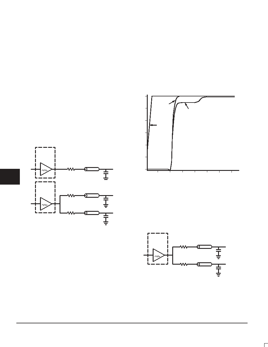
Figure 3. Single versus Dual Transmission Lines
14
IN
MPC9446
OUTPUT
BUFFER
RS = 36
ZO = 50
OutA
14
IN
MPC9446
OUTPUT
BUFFER
RS = 36
ZO = 50
OutB0
RS = 36
ZO = 50
OutB1
The waveform plots in Figure 4“Single versus Dual Line
Termination Waveforms” show the simulation results of an out-
put driving a single line versus two lines. In both cases the
drive capability of the MPC9446 output buffer is more than suf-
ficient to drive 50
transmission lines on the incident edge.
Note from the delay measurements in the simulations a delta
of only 43ps exists between the two differently loaded outputs.
This suggests that the dual line driving need not be used exclu-
sively to maintain the tight output-to-output skew of the
MPC9446. The output waveform in Figure 4“Single versus
Dual Line Termination Waveforms” shows a step in the wave-
form, this step is caused by the impedance mismatch seen
looking into the driver. The parallel combination of the 36
se-
ries resistor plus the output impedance does not match the
parallel combination of the line impedances. The voltage wave
launched down the two lines will equal:
VL = VS ( Z0 ÷ (RS+R0 +Z0))
Z0 = 50 || 50
RS = 36 || 36
R0 = 14
VL = 3.0 ( 25 ÷ (18+14+25)
= 1.31V
At the load end the voltage will double, due to the near unity
reflection coefficient, to 2.5V. It will then increment towards the
quiescent 3.0V in steps separated by one round trip delay (in
this case 4.0ns).
Figure 4. Single versus Dual Waveforms
TIME (nS)
VOL
TAGE
(V)
3.0
2.5
2.0
1.5
1.0
0.5
0
2
4
6
8
10
12
14
OutB
tD = 3.9386
OutA
tD = 3.8956
In
Since this step is well above the threshold region it will not
cause any false clock triggering, however designers may be
uncomfortable with unwanted reflections on the line. To better
match the impedances when driving multiple lines the situation
in Figure 5“Optimized Dual Line Termination” should be used.
In this case the series terminating resistors are reduced such
that when the parallel combination is added to the output buffer
impedance the line impedance is perfectly matched.
Figure 5. Optimized Dual Line Termination
14
MPC9446
OUTPUT
BUFFER
RS = 22
ZO = 50
RS = 22
ZO = 50
14
+ 22 k 22 = 50 k 50
25
= 25
F
re
e
sc
a
le
S
e
m
ic
o
n
d
u
c
to
r,
I
Freescale Semiconductor, Inc.
For More Information On This Product,
Go to: www.freescale.com
n
c
..
.
相关PDF资料 |
PDF描述 |
|---|---|
| MPC952FAR2 | LVCMOS/LVTTL SERIES, PLL BASED CLOCK DRIVER, 11 TRUE OUTPUT(S), 0 INVERTED OUTPUT(S), PQFP32 |
| MPC952FA | 952 SERIES, PLL BASED CLOCK DRIVER, 11 TRUE OUTPUT(S), 0 INVERTED OUTPUT(S), PQFP32 |
| MPC954DT | MPC900 SERIES, PLL BASED CLOCK DRIVER, 10 TRUE OUTPUT(S), 0 INVERTED OUTPUT(S), PDSO24 |
| MPC961PFA | 961 SERIES, PLL BASED CLOCK DRIVER, 17 TRUE OUTPUT(S), 0 INVERTED OUTPUT(S), PQFP32 |
| MPC962308D-4R2 | 962308 SERIES, PLL BASED CLOCK DRIVER, 8 TRUE OUTPUT(S), 0 INVERTED OUTPUT(S), PDSO16 |
相关代理商/技术参数 |
参数描述 |
|---|---|
| MPC9447 | 制造商:IDT 制造商全称:Integrated Device Technology 功能描述:3.3V/2.5V 1:9 LVCMOS Clock Fanout Buffer |
| MPC9447AC | 功能描述:时钟缓冲器 2.5 3.3V 250MHz Clock Generator RoHS:否 制造商:Texas Instruments 输出端数量:5 最大输入频率:40 MHz 传播延迟(最大值): 电源电压-最大:3.45 V 电源电压-最小:2.375 V 最大功率耗散: 最大工作温度:+ 85 C 最小工作温度:- 40 C 封装 / 箱体:LLP-24 封装:Reel |
| MPC9447ACR2 | 功能描述:时钟缓冲器 FSL 1-9 LVCMOS Fanout Buffer RoHS:否 制造商:Texas Instruments 输出端数量:5 最大输入频率:40 MHz 传播延迟(最大值): 电源电压-最大:3.45 V 电源电压-最小:2.375 V 最大功率耗散: 最大工作温度:+ 85 C 最小工作温度:- 40 C 封装 / 箱体:LLP-24 封装:Reel |
| MPC9447D | 制造商:MOTOROLA 制造商全称:Motorola, Inc 功能描述:3.3V/2.5V 1:9 LVCMOS Clock Fanout Buffer |
| MPC9447FA | 功能描述:时钟缓冲器 2.5 3.3V 275MHz Clock Generator RoHS:否 制造商:Texas Instruments 输出端数量:5 最大输入频率:40 MHz 传播延迟(最大值): 电源电压-最大:3.45 V 电源电压-最小:2.375 V 最大功率耗散: 最大工作温度:+ 85 C 最小工作温度:- 40 C 封装 / 箱体:LLP-24 封装:Reel |
发布紧急采购,3分钟左右您将得到回复。