- 您现在的位置:买卖IC网 > PDF目录45375 > MPC9456FA (MOTOROLA INC) LOW SKEW CLOCK DRIVER, 10 TRUE OUTPUT(S), 0 INVERTED OUTPUT(S), PQFP32 PDF资料下载
参数资料
| 型号: | MPC9456FA |
| 厂商: | MOTOROLA INC |
| 元件分类: | 时钟及定时 |
| 英文描述: | LOW SKEW CLOCK DRIVER, 10 TRUE OUTPUT(S), 0 INVERTED OUTPUT(S), PQFP32 |
| 封装: | 7 X 7 MM, PLASTIC, LQFP-32 |
| 文件页数: | 1/8页 |
| 文件大小: | 125K |
| 代理商: | MPC9456FA |
6
MOTOROLA
SEMICONDUCTOR TECHNICAL DATA
Order Number: MPC9456/D
Rev 1, 03/2002
MOTOROLA ADVANCED CLOCK DRIVERS DEVICE DATA
599
2.5V and 3.3V LVCMOS Clock
Fanout Buffer
The MPC9456 is a 2.5V and 3.3V compatible 1:10 clock distribution
buffer designed for low-voltage mid-range to high-performance telecom,
networking and computing applications. Both 3.3V, 2.5V and dual supply
voltages are supported for mixed-voltage applications. The MPC9456 of-
fers 10 low-skew outputs and a differential LVPECL clock input. The out-
puts are configurable and support 1:1 and 1:2 output to input frequency
ratios. The MPC9456 is specified for the extended temperature range of
–40 to 85
°C.
Features
Configurable 10 outputs LVCMOS clock distribution buffer
Compatible to single, dual and mixed 3.3V/2.5V voltage supply
Wide range output clock frequency up to 250 MHz
Designed for mid-range to high-performance telecom, networking and
computer applications
Supports high-performance differential clocking applications
Max. output skew of 200 ps (150 ps within one bank)
Selectable output configurations per output bank
Tristable outputs
32 ld LQFP package
Ambient operating temperature range of –40 to 85°C
Functional Description
The MPC9456 is a full static design supporting clock frequencies up to
250 MHz. The signals are generated and retimed on-chip to ensure mini-
mal skew between the three output banks.
Each of the three output banks can be individually supplied by 2.5V or 3.3V supporting mixed voltage applications. The FSELx
pins choose between division of the input reference frequency by one or two. The frequency divider can be set individually for
each of the three output banks. The MPC9456 can be reset and the outputs are disabled by deasserting the MR/OE pin (logic
high state). Asserting MR/OE will enable the outputs.
All control inputs accept LVCMOS signals while the outputs provide LVCMOS compatible levels with the capability to drive
terminated 50
transmission lines. The clock input is low voltage PECL compatible for differential clock distribution support.
Please consult the MPC9446 specification for a full CMOS compatible device. For series terminated transmission lines, each of
the MPC9456 outputs can drive one or two traces giving the devices an effective fanout of 1:20. The device is packaged in a 7x7
mm2 32-lead LQFP package.
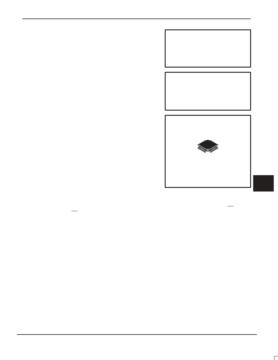
FA SUFFIX
LQFP PACKAGE
CASE 873A
MPC9456
LOW VOLTAGE SINGLE OR
DUAL SUPPLY 2.5V AND 3.3V
LVCMOS CLOCK
DISTRIBUTION BUFFER
相关PDF资料 |
PDF描述 |
|---|---|
| MPC955FAR2 | 300 MHz, PROC SPECIFIC CLOCK GENERATOR, PQFP32 |
| MPC972FAR2 | 125 MHz, PROC SPECIFIC CLOCK GENERATOR, PQFP52 |
| MPC972FAR2 | 125 MHz, PROC SPECIFIC CLOCK GENERATOR, PQFP52 |
| MPC972FAR2 | 125 MHz, PROC SPECIFIC CLOCK GENERATOR, PQFP52 |
| MPC972FA | 125 MHz, PROC SPECIFIC CLOCK GENERATOR, PQFP52 |
相关代理商/技术参数 |
参数描述 |
|---|---|
| MPC946 | 制造商:MOTOROLA 制造商全称:Motorola, Inc 功能描述:LOW VOLTAGE 1:10 CMOS CLOCK DRIVER |
| MPC947 | 制造商:MOTOROLA 制造商全称:Motorola, Inc 功能描述:LOW VOLTAGE 1:9 CLOCK DISTRIBUTION CHIP |
| MPC947FA | 制造商:Freescale Semiconductor 功能描述: |
| MPC948 | 制造商:MOTOROLA 制造商全称:Motorola, Inc 功能描述:LOW VOLTAGE 1:12 CLOCK DISTRIBUTION CHIP |
| MPC948FA | 制造商:Motorola Inc 功能描述:TWELVE DISTRIBUTED-OUTPUT CLOCK DRIVER, 32 Pin, Plastic, QFP |
发布紧急采购,3分钟左右您将得到回复。