- 您现在的位置:买卖IC网 > PDF目录26839 > MPC962305D-1 (FREESCALE SEMICONDUCTOR INC) 962305 SERIES, PLL BASED CLOCK DRIVER, 8 TRUE OUTPUT(S), 0 INVERTED OUTPUT(S), PDSO8 PDF资料下载
参数资料
| 型号: | MPC962305D-1 |
| 厂商: | FREESCALE SEMICONDUCTOR INC |
| 元件分类: | 时钟及定时 |
| 英文描述: | 962305 SERIES, PLL BASED CLOCK DRIVER, 8 TRUE OUTPUT(S), 0 INVERTED OUTPUT(S), PDSO8 |
| 封装: | 0.150 INCH, SOIC-8 |
| 文件页数: | 4/6页 |
| 文件大小: | 110K |
| 代理商: | MPC962305D-1 |
MPC962305
510
FREESCALE SEMICONDUCTOR ADVANCED CLOCK DRIVERS DEVICE DATA
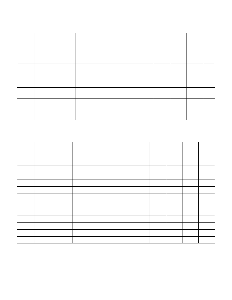
Table 7. Switching Characteristics for MPC962305-1 and MPC962309-1 Industrial Temperature Devices1
1.
All parameters are specified with loaded outputs.
Parameter
Name
Test Conditions
Min
Typ
Max
Unit
t1
Output Frequency
30-pF load
10-pF load
10
100
133.33
MHz
Duty Cycle2 = t2 ÷ t1
2.
Parameter is guaranteed by design and characterization. Not 100% tested in production.
Measured at 1.4 V, FOUT = 66.67 MHz
40.0
50.0
60.0
%
t3
Rise Time2
Measured between 0.8 V and 2.0 V
2.50
ns
t4
Fall Time2
Measured between 0.8 V and 2.0 V
2.50
ns
t5
Output to Output Skew2
All outputs equally loaded
250
ps
t6A
Delay, REF Rising Edge to
CLKOUT Rising Edge2
Measured at VDD/2
0
±350
ps
t6B
Delay, REF Rising Edge to
CLKOUT Rising Edge2
Measured at VDD/2. Measured in PLL Bypass Mode,
MPC962309 device only
15
8.7
ns
t7
Device to Device Skew2
Measured at VDD/2 on the CLKOUT pins of devices
0700
ps
tJ
Cycle to Cycle Jitter2
Measured at 66.67 MHz, loaded outputs
200
ps
tLOCK
PLL Lock Time2
Stable power supply, valid clock presented on REF pin
1.0
ms
Table 8. Switching Characteristics for MPC962305-1H and MPC962309-1H Industrial Temperature Devices1
1.
All parameters are specified with loaded outputs.
Parameter
Name
Test Conditions
Min
Typ
Max
Unit
t1
Output Frequency
30-pF load
10-pF load
10
100
133.33
MHz
Duty Cycle2 = t2
÷ t1
2.
Parameter is guaranteed by design and characterization. Not 100% tested in production.
Measured at 1.4 V, FOUT = 66.67 MHz
40.0
50.0
60.0
%
Duty Cycle2 = t2
÷ t1
Measured at 1.4 V, FOUT < 50 MHz
45.0
55.0
%
t3
Rise Time2
Measured between 0.8 V and 2.0 V
1.50
ns
t4
Fall Time2
Measured between 0.8 V and 2.0 V
1.50
ns
t5
Output to Output Skew2
All outputs equally loaded
250
ps
t6A
Delay, REF Rising Edge to
CLKOUT Rising Edge2
Measured at VDD/2
0
±350
ps
t6B
Delay, REF Rising Edge to
CLKOUT Rising Edge2
Measured at VDD/2. Measured in PLL Bypass Mode,
MPC962309 device only
15
8.7
ns
t7
Device to Device Skew2
Measured at VDD/2 on the CLKOUT pins of devices
0700
ps
t8
Output Slew Rate2
Measured between 0.8 V and 2.0 V using Test Circuit #2
1V/ns
tJ
Cycle to Cycle Jitter2
Measured at 66.67 MHz, loaded outputs
200
ps
tLOCK
PLL Lock Time2
Stable power supply, valid clock presented on REF pin
1.0
ms
相关PDF资料 |
PDF描述 |
|---|---|
| MPC962309DT-1H | 962309 SERIES, PLL BASED CLOCK DRIVER, 8 TRUE OUTPUT(S), 0 INVERTED OUTPUT(S), PDSO16 |
| MPC962309D-1R2 | 962309 SERIES, PLL BASED CLOCK DRIVER, 8 TRUE OUTPUT(S), 0 INVERTED OUTPUT(S), PDSO16 |
| MPC962305EF-1HR2 | 962305 SERIES, PLL BASED CLOCK DRIVER, 8 TRUE OUTPUT(S), 0 INVERTED OUTPUT(S), PDSO8 |
| MPC962309EF-1H | 962309 SERIES, PLL BASED CLOCK DRIVER, 8 TRUE OUTPUT(S), 0 INVERTED OUTPUT(S), PDSO16 |
| MPC962305D-1R2 | 962305 SERIES, PLL BASED CLOCK DRIVER, 4 TRUE OUTPUT(S), 0 INVERTED OUTPUT(S), PDSO8 |
相关代理商/技术参数 |
参数描述 |
|---|---|
| MPC962305D-1H | 功能描述:IC CLOCK BUFFER 1:5 8-SOIC RoHS:否 类别:集成电路 (IC) >> 时钟/计时 - 时钟发生器,PLL,频率合成器 系列:- 标准包装:39 系列:- 类型:* PLL:带旁路 输入:时钟 输出:时钟 电路数:1 比率 - 输入:输出:1:10 差分 - 输入:输出:是/是 频率 - 最大:170MHz 除法器/乘法器:无/无 电源电压:2.375 V ~ 3.465 V 工作温度:0°C ~ 70°C 安装类型:* 封装/外壳:* 供应商设备封装:* 包装:* |
| MPC962305D-1HR2 | 制造商:MOTOROLA 制造商全称:Motorola, Inc 功能描述:Low-Cost 3.3 V Zero Delay Buffer |
| MPC962305D-1R2 | 制造商:MOTOROLA 制造商全称:Motorola, Inc 功能描述:Low-Cost 3.3 V Zero Delay Buffer |
| MPC962305DT-1H | 功能描述:IC CLOCK BUFFER 1:5 8-TSSOP RoHS:否 类别:集成电路 (IC) >> 时钟/计时 - 时钟发生器,PLL,频率合成器 系列:- 标准包装:39 系列:- 类型:* PLL:带旁路 输入:时钟 输出:时钟 电路数:1 比率 - 输入:输出:1:10 差分 - 输入:输出:是/是 频率 - 最大:170MHz 除法器/乘法器:无/无 电源电压:2.375 V ~ 3.465 V 工作温度:0°C ~ 70°C 安装类型:* 封装/外壳:* 供应商设备封装:* 包装:* |
| MPC962305DT-1HR2 | 制造商:MOTOROLA 制造商全称:Motorola, Inc 功能描述:Low-Cost 3.3 V Zero Delay Buffer |
发布紧急采购,3分钟左右您将得到回复。