- 您现在的位置:买卖IC网 > PDF目录9620 > MPC96877VKR2 (IDT, Integrated Device Technology Inc)IC CLK DRIVER 1:10 SDRAM 52-BGA PDF资料下载
参数资料
| 型号: | MPC96877VKR2 |
| 厂商: | IDT, Integrated Device Technology Inc |
| 文件页数: | 10/13页 |
| 文件大小: | 0K |
| 描述: | IC CLK DRIVER 1:10 SDRAM 52-BGA |
| 标准包装: | 2,500 |
| 类型: | 时钟缓冲器/驱动器,多路复用器 |
| PLL: | 是 |
| 主要目的: | 存储器,DDR2,SDRAM |
| 输入: | 时钟 |
| 输出: | SSTL-18 |
| 电路数: | 1 |
| 比率 - 输入:输出: | 1:10 |
| 差分 - 输入:输出: | 是/是 |
| 频率 - 最大: | 340MHz |
| 电源电压: | 1.7 V ~ 1.9 V |
| 工作温度: | 0°C ~ 70°C |
| 安装类型: | 表面贴装 |
| 封装/外壳: | 52-BGA |
| 包装: | 带卷 (TR) |
MPC96877
552
FREESCALE SEMICONDUCTOR ADVANCED CLOCK DRIVERS DEVICE DATA
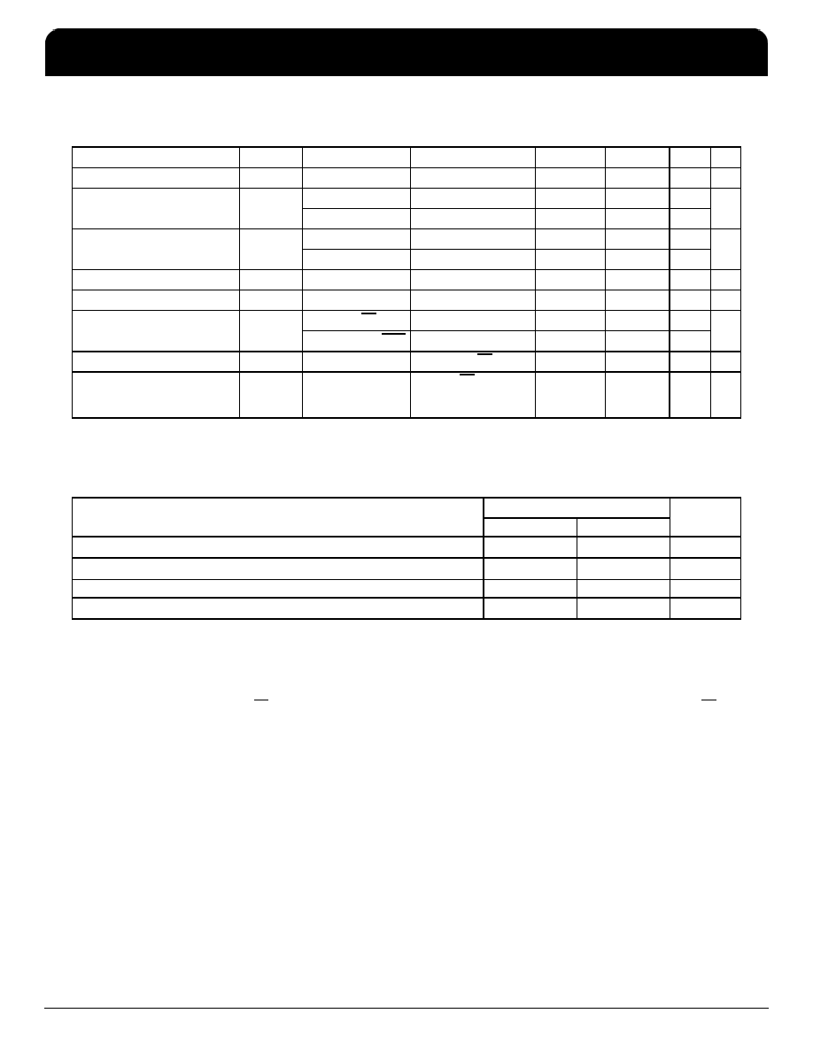
1. Total IDD = IDDQ + IADD = FCK* CPD * VDDQ, solving for CPD = (IDDQ + IADD)/(FCK * VDDQ) where FCK is the input Frequency, VDDQ is the power
supply and CPD is the Power Dissipation Capacitance.
Table 5. Electrical Characteristics Over Recommended Free-Air Operating Temperature Range
Description
Parameter
Affected Pins
Test Conditions
AVDD, VDDQ
Min
Max
Unit
All inputs
VIK
II = –18mA
1.7 V
–1.2
V
High output voltage
VOH
IOH = –100 A
1.7 to 1.9 V
VDDQ –0.2
V
IOH = –9 mA
1.7 V
1.1
Low output voltage
VOL
IOL = 100 A
1.7 to 1.9 V
0.1
V
IOL = 9 mA
1.7 V
0.6
Output disable current
IODL
OE = L, VODL = 100 mV
1.7 V
100
A
Output differential voltage
VOD
1.7 V
0.5
V
Input leakage current
II
CK, CK
VI = VDDQ or GND
1.9 V
± 250
A
OE, OS, FBIN, FBIN
VI = VDDQ or GND
1.9 V
± 10
Static supply current IDDQ + IADD
IDDLD
CK and CK = L
1.9 V
500
A
Dynamic Supply current
IDDQ + IADD, see Note 1 for CPD
calculation
IDD
CK and CK = 270 MHz
all outputs open
1.9 V
300
mA
Table 6. Timing Requirements Over Recommended Free-Air Operating Temperature Range
Timing Requirements
AVDD, VDDQ = 1.8 V ± 0.1 V
Unit
Min
Max
Operating clock frequency1, 2
1. The PLL must be able to handle spread spectrum induced skew.
2. Operating clock frequency indicates a range over which the PLL must be able to lock, but in which it is not required to meet the other timing
parameters. (Used for low speed system debug.)
125
340
MHz
Application clock frequency1, 3
3. Application clock frequency indicates a range over which the PLL must meet all timing parameters.
160
340
MHz
Input clock duty cycle
40
60
%
Stabilization time4
4. Stabilization time is the time required for the integrated PLL circuit to obtain phase lock of its feedback signal to its reference signal after power
up. During normal operation, the stabilization time is also the time required for the integrated PLL circuit to obtain phase lock of its feedback signal
to its reference signal when CK and CK go to a logic low state, enter the power-down mode and later return to active operation. CK and CK may
be left floating after they have been driven low for one complete clock cycle.
15
s
MPC96877
1.8 V PLL 1:10 Differential SDRAM Clock Driver
NETCOM
IDT 1.8 V PLL 1:10 Differential SDRAM Clock Driver
Freescale Timing Solutions Organization has been acquired by Integrated Device Technology, Inc
MPC96877
6
相关PDF资料 |
PDF描述 |
|---|---|
| MS27656T25F29SB | CONN RCPT 29POS WALL MNT W/SCKT |
| VI-BWV-MW-F1 | CONVERTER MOD DC/DC 5.8V 100W |
| MS27656T25F29SC | CONN RCPT 29POS WALL MNT W/SCKT |
| EL1529ILZ | IC LINE DRVR DUAL ADSL2++ 24-QFN |
| EL1529IL-T7 | IC LINE DRVR DUAL ADSL2++ 24-QFN |
相关代理商/技术参数 |
参数描述 |
|---|---|
| MPC970 | 制造商:MOTOROLA 制造商全称:Motorola, Inc 功能描述:LOW VOLTAGE PLL CLOCK DRIVER |
| MPC972 | 制造商:Motorola Inc 功能描述: |
| MPC972FA | 制造商:Freescale Semiconductor 功能描述: |
| MPC972H10 F44A WAF | 制造商:Motorola Inc 功能描述: |
| MPC973 | 制造商:MOTOROLA 制造商全称:Motorola, Inc 功能描述:LOW VOLTAGE PLL CLOCK DRIVER |
发布紧急采购,3分钟左右您将得到回复。