- 您现在的位置:买卖IC网 > PDF目录29137 > MPC974FAR2 (INTEGRATED DEVICE TECHNOLOGY INC) 974 SERIES, PLL BASED CLOCK DRIVER, 14 TRUE OUTPUT(S), 0 INVERTED OUTPUT(S), PQFP52 PDF资料下载
参数资料
| 型号: | MPC974FAR2 |
| 厂商: | INTEGRATED DEVICE TECHNOLOGY INC |
| 元件分类: | 时钟及定时 |
| 英文描述: | 974 SERIES, PLL BASED CLOCK DRIVER, 14 TRUE OUTPUT(S), 0 INVERTED OUTPUT(S), PQFP52 |
| 封装: | PLASTIC, LQFP-52 |
| 文件页数: | 4/6页 |
| 文件大小: | 294K |
| 代理商: | MPC974FAR2 |
MPC974
MOTOROLA ADVANCED CLOCK DRIVERS DEVICE DATA
213
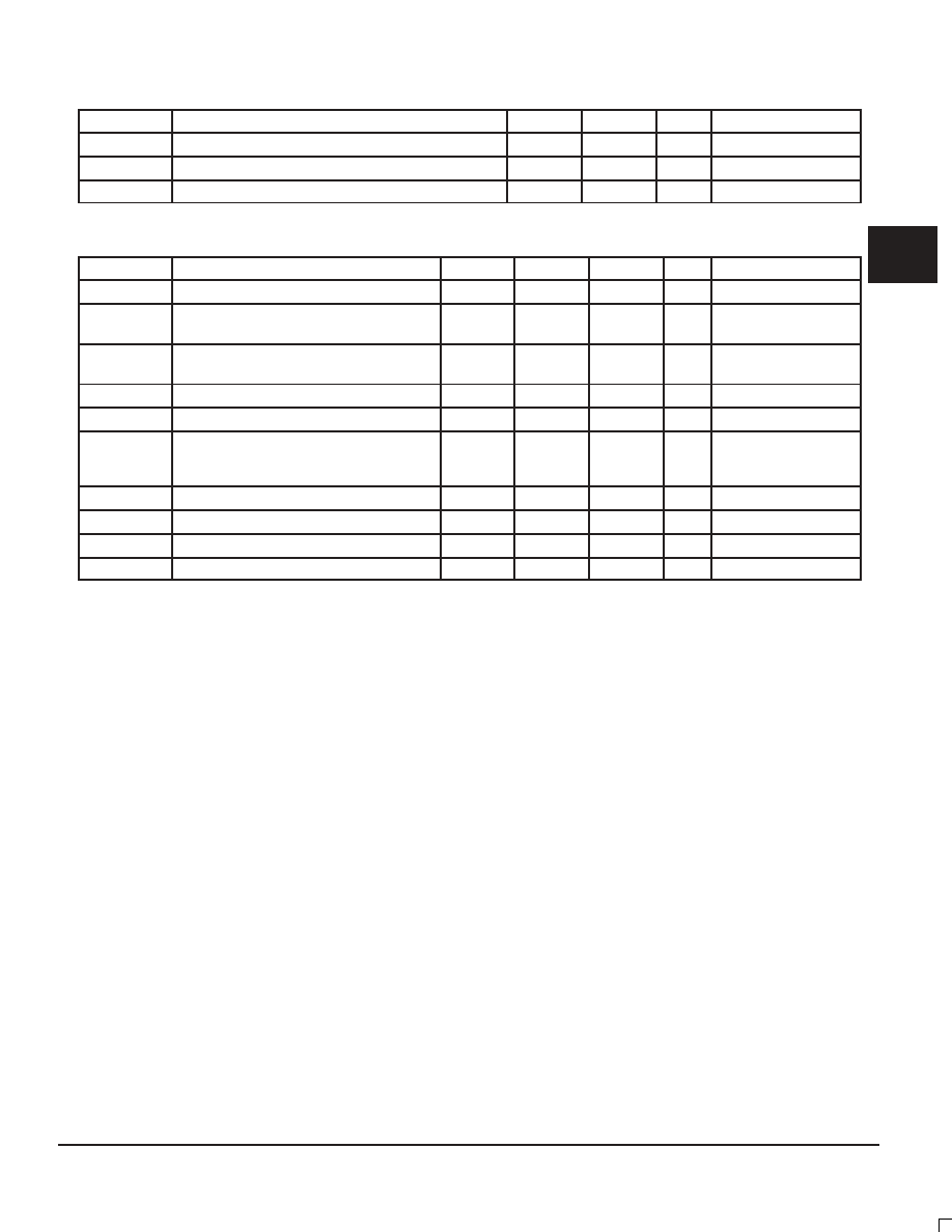
PLL INPUT REFERENCE CHARACTERISTICS (TA = 0 to 70°C)
Symbol
Characteristic
Min
Max
Unit
Condition
tr, tf
TCLK Input Rise/Falls
3.0
ns
fref
Reference Input Frequency
Note 3.
MHz
frefDC
Reference Input Duty Cycle
25
75
%
3. Input reference frequency is limited by the divider selection and the VCO lock range.
AC CHARACTERISTICS (TA = 0° to 70°C, VCC = 3.3V ±5%)
Symbol
Characteristic
Min
Typ
Max
Unit
Condition
tr, tf
Output Rise/Fall Time
0.15
1.5
ns
0.8 to 2.0V, Note 4.
tpw
Output Duty Cycle
tCYCLE/2
–800
tCYCLE/2
±500
tCYCLE/2
+800
ps
Note 4.
fVCO
PLL VCO Lock Range
fseln, fselFBn =
÷4 to ÷12
200
500
MHz
Note 5.
tpd
SYNC to Feedback Propagation Delay
–250
100
ps
Notes 4., 6.
tos
Output-to-Output Skew
350
ps
Note 4.
fmax
Maximum Output Frequency
Q (
÷2)
Q (
÷4)
Q (
÷6)
125
63
42
MHz
VCO_Sel = 0
tPZL
Output Enable Time
2
10
ns
Note 4.
tPLZ, tPHZ
Output Disable Time
2
10
ns
Note 4.
tjitter
Cycle–to–Cycle Jitter (Peak–to–Peak)
±100
ps
Note 4.
tlock
Maximum PLL Lock Time
10
ms
4. 50
transmission lines terminated to VCC/2.
5. The PLL will be unstable if the total divide between the VCO and the feedback pin is less < 8. VCO_SEL = ‘0’, fsela or fselb = ‘0’ cannot be used
for the PLL feedback signal.
6. tpd is specified for 50MHz input reference. The window will shrink/grow proportionally from the minimum limit with shorter/longer input reference
periods. The tpd does not include jitter.
APPLICATIONS INFORMATION
Programming the MPC974
The MPC974 clock driver outputs can be configured into
several frequency relationships, in addition the external feed-
back option allows for a great deal of flexibility in establishing
unique input–to–output frequency relationships. The output di-
viders for the four output groups allows the user to configure
the outputs into 1:1, 2:1, 3:2 and 3:2:1 frequency ratios. The
use of even dividers ensures that the output duty cycle is al-
ways 50%. Function Table 1 illustrates the various output con-
figurations, the table describes the outputs using the VCO fre-
quency as a reference. As an example for a 3:2:1 relationship
the Qa outputs would be set at VCO/2, the Qb’s and Qc’s at
VCO/4 and the Qd’s at VCO/6. These settings will provide out-
put frequencies with a 3:2:1 relationship.
The division settings establish the output relationship, but
one must still ensure that the VCO will be stable given the
frequency of the outputs desired. The VCO lock range can be
found in the specification tables. The feedback frequency
should be used to situate the VCO into a frequency range in
which the PLL will be stable. The design of the PLL is such that
for output frequencies between 10 and 125MHz the MPC974
can generally be configured into a stable region.
The relationship between the input reference and the output
frequency is also very flexible. The separate PLL feedback
output allows for a wide range of output vs input frequency
relationships. Function Table 1 can be used to identify the po-
tential relationships available. Figure 3 illustrates several pro-
gramming possibilities, although not exhaustive it is represen-
tative of the potential applications.
Using the MPC974 as a Zero Delay Buffer
The external feedback option of the MPC974 clock driver
allows for its use as a zero delay buffer. By using one of the
outputs as a feedback to the PLL the propagation delay
through the device is near zero. The PLL works to align the
output edge with the input reference edge thus producing a
near zero delay. The static phase offset is a function of the
input reference frequency of the MPC974. The Tpd of the de-
vice is specified in the specification tables.
To minimize part–to–part skew the external feedback option
again should be used. The PLL in the MPC974 decouples the
delay of the device from the propagation delay variations of the
internal gates. From the specification table one sees a Tpd
variation of only
±150ps, thus for multiple devices under identi-
cal configurations the part–to–part skew will be around 850ps
(300ps for Tpd variation plus 350ps output–to–output skew
plus 200ps for jitter). To minimize this value, the highest pos-
sible reference frequencies should be used. Higher reference
frequencies will minimize both the tpd parameter as well as the
input to output jitter.
2
F
re
e
sc
a
le
S
e
m
ic
o
n
d
u
c
to
r,
I
Freescale Semiconductor, Inc.
For More Information On This Product,
Go to: www.freescale.com
n
c
..
.
相关PDF资料 |
PDF描述 |
|---|---|
| MPC974FA | 974 SERIES, PLL BASED CLOCK DRIVER, 14 TRUE OUTPUT(S), 0 INVERTED OUTPUT(S), PQFP52 |
| MPC974FA | 974 SERIES, PLL BASED CLOCK DRIVER, 14 TRUE OUTPUT(S), 0 INVERTED OUTPUT(S), PQFP52 |
| MPC9773AE | 9773 SERIES, PLL BASED CLOCK DRIVER, 12 TRUE OUTPUT(S), 0 INVERTED OUTPUT(S), PQFP52 |
| MPC97H74AER2 | 97H SERIES, PLL BASED CLOCK DRIVER, 14 TRUE OUTPUT(S), 0 INVERTED OUTPUT(S), PQFP52 |
| MPC97H74FAR2 | 97H SERIES, PLL BASED CLOCK DRIVER, 14 TRUE OUTPUT(S), 0 INVERTED OUTPUT(S), PQFP52 |
相关代理商/技术参数 |
参数描述 |
|---|---|
| MPC9772 | 制造商:MOTOROLA 制造商全称:Motorola, Inc 功能描述:3.3V 1:12 LVCMOS PLL Clock Generator |
| MPC9772AE | 功能描述:锁相环 - PLL 2.5 3.3V 250MHz Clock Generator RoHS:否 制造商:Silicon Labs 类型:PLL Clock Multiplier 电路数量:1 最大输入频率:710 MHz 最小输入频率:0.002 MHz 输出频率范围:0.002 MHz to 808 MHz 电源电压-最大:3.63 V 电源电压-最小:1.71 V 最大工作温度:+ 85 C 最小工作温度:- 40 C 封装 / 箱体:QFN-36 封装:Tray |
| MPC9772AER2 | 功能描述:时钟发生器及支持产品 FSL 1-12 LVCMOS PLL Clock Generator, xta RoHS:否 制造商:Silicon Labs 类型:Clock Generators 最大输入频率:14.318 MHz 最大输出频率:166 MHz 输出端数量:16 占空比 - 最大:55 % 工作电源电压:3.3 V 工作电源电流:1 mA 最大工作温度:+ 85 C 安装风格:SMD/SMT 封装 / 箱体:QFN-56 |
| MPC9772FA | 功能描述:锁相环 - PLL 3.3V 240MHz Clock Generator RoHS:否 制造商:Silicon Labs 类型:PLL Clock Multiplier 电路数量:1 最大输入频率:710 MHz 最小输入频率:0.002 MHz 输出频率范围:0.002 MHz to 808 MHz 电源电压-最大:3.63 V 电源电压-最小:1.71 V 最大工作温度:+ 85 C 最小工作温度:- 40 C 封装 / 箱体:QFN-36 封装:Tray |
| MPC9772FAR2 | 功能描述:时钟发生器及支持产品 FSL 1-12 LVCMOS PLL Clock Generator, xta RoHS:否 制造商:Silicon Labs 类型:Clock Generators 最大输入频率:14.318 MHz 最大输出频率:166 MHz 输出端数量:16 占空比 - 最大:55 % 工作电源电压:3.3 V 工作电源电流:1 mA 最大工作温度:+ 85 C 安装风格:SMD/SMT 封装 / 箱体:QFN-56 |
发布紧急采购,3分钟左右您将得到回复。