- 您现在的位置:买卖IC网 > PDF目录29137 > MPC97H74AER2 (FREESCALE SEMICONDUCTOR INC) 97H SERIES, PLL BASED CLOCK DRIVER, 14 TRUE OUTPUT(S), 0 INVERTED OUTPUT(S), PQFP52 PDF资料下载
参数资料
| 型号: | MPC97H74AER2 |
| 厂商: | FREESCALE SEMICONDUCTOR INC |
| 元件分类: | 时钟及定时 |
| 英文描述: | 97H SERIES, PLL BASED CLOCK DRIVER, 14 TRUE OUTPUT(S), 0 INVERTED OUTPUT(S), PQFP52 |
| 封装: | LEAD FREE, LQFP-52 |
| 文件页数: | 9/12页 |
| 文件大小: | 240K |
| 代理商: | MPC97H74AER2 |
Advanced Clock Driver Devices
6
Freescale Semiconductor
MPC97H74
APPLICATIONS INFORMATION
MPC97H74 Configurations
Configuring the MPC97H74 amounts to properly
configuring the internal dividers to produce the desired output
frequencies. The output frequency can be represented by
this formula:
where fREF is the reference frequency of the selected input
clock source (CCLKO or CCLK1), M is the PLL feedback
divider and N is a output divider. M is configured by the
FSEL_FB[0:1] and N is individually configured for each
output bank by the FSEL_A, FSEL_B and FSEL_C inputs.
The reference frequency fREF and the selection of the
feedback-divider M is limited by the specified VCO frequency
range. fREF and M must be configured to match the VCO
frequency range of 200 to 500 MHz (210 to 450 MHz for
industrial temperature range) in order to achieve stable PLL
operation:
fVCO,MIN ≤ (fREF × VCO_SEL × M) ≤ fVCO,MAX
The PLL post-divider VCO_SEL is either a divide-by-two
or a divide-by-four and can be used to situate the VCO into
the specified frequency range. This divider is controlled by
the VCO_SEL pin. VCO_SEL effectively extends the usable
input frequency range while it has no effect on the output to
reference frequency ratio. The output frequency for each
bank can be derived from the VCO frequency and the output
divider:
fQA[4:0] = fVCO ÷ (VCO_SEL × NA)
fQB[4:0] = fVCO ÷ (VCO_SEL × NB)
fQC[3:0] = fVCO ÷ (VCO_SEL × NC)
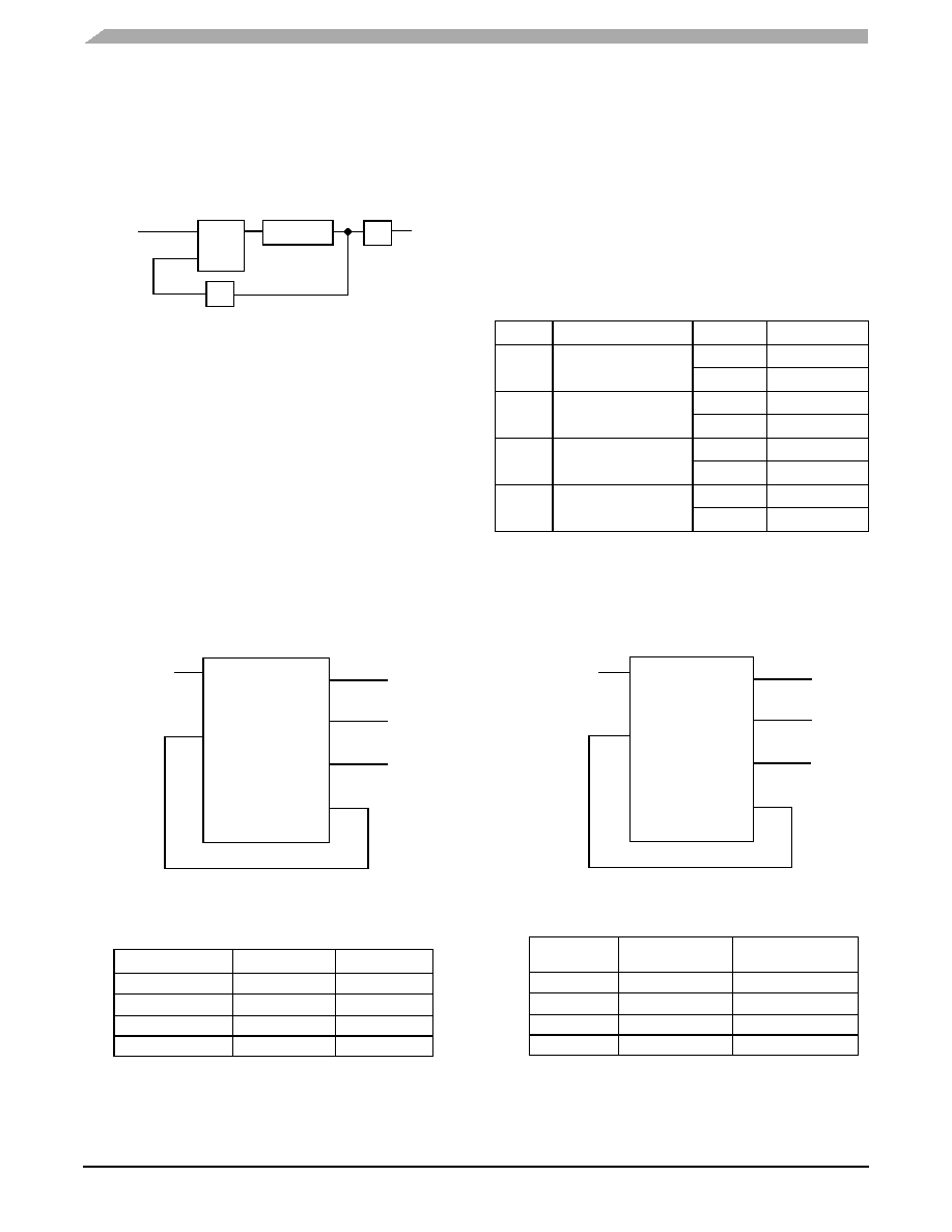
Table 10 shows the various PLL feedback and output
dividers. The output dividers for the three output banks allow
the user to configure the outputs into 1:1, 2:1, 3:2, and 3:2:1
configurations for the MPC97H74:
fOUT = fREF × M ÷ N
fREF
PLL
÷VCO_SEL
÷ N
fOUT
÷ M
Table 10. MPC97H74 Dividers
Divider
Function
VCO_SEL
Values
M
PLL feedback
FSEL_FB[0:1]
÷ 2
8, 12, 16, 24
÷ 4
16, 24, 32, 48
NA
Bank A Output Divider
FSEL_A
÷ 2
4, 8
÷ 4
8, 16
NB
Bank B Output Divider
FSEL_B
÷ 2
4, 8
÷ 4
8, 16
NC
Bank C Output Divider
FSEL_C
÷ 2
8, 12
÷ 4
16, 24
Figure 3. Example Configuration
Figure 4. Example Configuration
MPC97H74
fREF = 20.83 MHz
125 MHz
62.5 MHz
20.83 MHz (Feedback)
62.5 MHz
CCLK0
VCO_SEL
FSEL_A
FSEL_B
FSEL_C
FSEL_FB[1:0]
QA[4:0]
QB[4:0]
QC[3:0]
QFB
CCLK1
CCLK_SEL
FB_IN
0
1
0
11
0
Frequency Range
Min
Max
Input
8.33 MHz
20.83 MHz
QA outputs
50 MHz
125 MHz
QB outputs
25 MHz
62.5 MHz
QC outputs
25 MHz
62.5 MHz
MPC97H74
fREF = 25 MHz
100 MHz
50 MHz
25 MHz (Feedback)
33.3 MHz
CCLK0
VCO_SEL
FSEL_A
FSEL_B
FSEL_C
FSEL_FB[1:0]
QA[4:0]
QB[4:0]
QC[3:0]
QFB
CCLK1
CCLK_SEL
FB_IN
0
1
01
0
MPC97H74 example configuration (feedback of
QFB = 25 MHz, VCO_SEL =
÷ 2, M = 8, N
A = 2,
NB = 4, NC = 6, fVCO = 400 MHz).
Frequency
Range
TA = 0°C to +70°C TA = -40°C to +85°C
Input
12.50 - 31.25 MHz 13.125 - 28.125 MHz
QA outputs
50.00 - 125.0 MHz
52.50 - 112.5 MHz
QB outputs
25.00 - 62.50 MHz
26.25 - 56.25 MHz
QC outputs
16.67 - 41.67 MHz
17.50 - 37.50 MHz
MPC97H74 example configuration (feedback of
QFB = 20.83 MHz, VCO_SEL =
÷ 2, M = 12, N
A = 2,
NB = 4, NC = 4, fVCO = 500 MHz). TA = 0°C to 70°C
相关PDF资料 |
PDF描述 |
|---|---|
| MPC97H74FAR2 | 97H SERIES, PLL BASED CLOCK DRIVER, 14 TRUE OUTPUT(S), 0 INVERTED OUTPUT(S), PQFP52 |
| MPC97H74FA | 97H SERIES, PLL BASED CLOCK DRIVER, 14 TRUE OUTPUT(S), 0 INVERTED OUTPUT(S), PQFP52 |
| MPC9893FAR2 | 9893 SERIES, PLL BASED CLOCK DRIVER, 12 TRUE OUTPUT(S), 0 INVERTED OUTPUT(S), PQFP48 |
| MPC991FAR2 | PLL BASED CLOCK DRIVER, 13 TRUE OUTPUT(S), 0 INVERTED OUTPUT(S), PQFP52 |
| MPC991FAR2 | PLL BASED CLOCK DRIVER, 13 TRUE OUTPUT(S), 0 INVERTED OUTPUT(S), PQFP52 |
相关代理商/技术参数 |
参数描述 |
|---|---|
| MPC97H74FA | 功能描述:IC PLL CLK GENERATOR 1:14 52LQFP RoHS:否 类别:集成电路 (IC) >> 时钟/计时 - 时钟发生器,PLL,频率合成器 系列:- 标准包装:39 系列:- 类型:* PLL:带旁路 输入:时钟 输出:时钟 电路数:1 比率 - 输入:输出:1:10 差分 - 输入:输出:是/是 频率 - 最大:170MHz 除法器/乘法器:无/无 电源电压:2.375 V ~ 3.465 V 工作温度:0°C ~ 70°C 安装类型:* 封装/外壳:* 供应商设备封装:* 包装:* |
| MPC980 | 制造商:MOTOROLA 制造商全称:Motorola, Inc 功能描述:DUAL 3.3V PLL CLOCK GENERATOR |
| MPC9817 | 制造商:FREESCALE 制造商全称:Freescale Semiconductor, Inc 功能描述:Clock Generator for PowerQUICC and PowerPC Microprocessors and Microcontrollers |
| MPC9817EN | 功能描述:时钟发生器及支持产品 FSL 1-5 PwrQUICC/Pwr PC Clk Gen, RoHS:否 制造商:Silicon Labs 类型:Clock Generators 最大输入频率:14.318 MHz 最大输出频率:166 MHz 输出端数量:16 占空比 - 最大:55 % 工作电源电压:3.3 V 工作电源电流:1 mA 最大工作温度:+ 85 C 安装风格:SMD/SMT 封装 / 箱体:QFN-56 |
| MPC9817ENR2 | 功能描述:时钟发生器及支持产品 FSL 1-5 PwrQUICC/Pwr PC Clk Gen, RoHS:否 制造商:Silicon Labs 类型:Clock Generators 最大输入频率:14.318 MHz 最大输出频率:166 MHz 输出端数量:16 占空比 - 最大:55 % 工作电源电压:3.3 V 工作电源电流:1 mA 最大工作温度:+ 85 C 安装风格:SMD/SMT 封装 / 箱体:QFN-56 |
发布紧急采购,3分钟左右您将得到回复。