- 您现在的位置:买卖IC网 > PDF目录95995 > MPC992FA (INTEGRATED DEVICE TECHNOLOGY INC) 375 MHz, PROC SPECIFIC CLOCK GENERATOR, PQFP32 PDF资料下载
参数资料
| 型号: | MPC992FA |
| 厂商: | INTEGRATED DEVICE TECHNOLOGY INC |
| 元件分类: | 时钟产生/分配 |
| 英文描述: | 375 MHz, PROC SPECIFIC CLOCK GENERATOR, PQFP32 |
| 封装: | LQFP-32 |
| 文件页数: | 1/8页 |
| 文件大小: | 312K |
| 代理商: | MPC992FA |
Low Voltage PECL PLL
Clock Driver
The MPC992 is a 3.3V compatible, PLL based PECL clock generator and
distributor. The fully differential design ensures optimum skew and PLL jitter
performance. The performance of the device makes the MPC992 ideal for
work s tations , main frame computer, telec ommunic ation and
instrumentation applications. The device offers a crystal oscillator or a
differential PECL reference clock input to provide flexibility in the reference
clock interface. All of the control signals to the MPC992 are LVTTL
compatible inputs.
Fully Integrated PLL
Output Frequency of up to 400MHz
PECL Clock Inputs and Outputs
Operates from a 3.3V VCC Supply
Output Frequency Configurable
32 TQFP Packaging
±25ps Cycle–Cycle Jitter
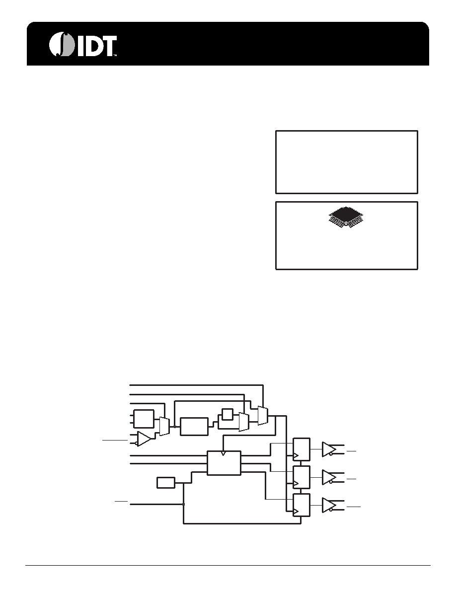
The MPC992 offers two banks of outputs which can be configured into
four different relationships. The output banks can be configured into 2:1,
3:1, 3:2 and 5:2 ratios to provide a wide variety of potential frequency
outputs. In addition to these two banks of outputs a synchronization output is also offered. The SYNC output will provide
information as to the time when the two output banks will transition positively in phase. This information can be important when the
odd ratios are used as it provides for a baseline point in the system timing. The SYNC output will pulse high for one Qa clock
period, centered on the rising Qa clock edge four edges prior to the Qb synchronous edge. The relationship is illustrated in the
timing diagrams in the data sheet.
The MPC992 offers several features to aid in system debug and test. The PECL reference input pins can be interfaced to a test
signal and the PLL can be bypassed to allow the designer to drive the MPC992 outputs directly. This allows for single stepping in
a system functional debug mode. In addition an overriding reset is provided which will force all of the Q outputs LOW upon
assertion.
The MPC992 is packaged in a 32–lead TQFP package to optimize both performance and board density.
Qan
(x4)
Qbn
(x3)
SYNC
(x1)
Frequency
Generator
PLL_EN
PECL_CLK
XTAL_SEL
XTAL
OSC
XTAL1
XTAL2
VCO_SEL
Integrated
PLL
x2
FSEL0
FSEL1
POR
Reset
MPC992 LOGIC DIAGRAM
1
0
1
0
1
Order Number: MPC992/D
Rev. 2, 08/2001
MOTOROLA
SEMICONDUCTOR TECHNICAL DATA
Motorola, Inc. 2001
t
MPC992
LOW VOLTAGE
PLL CLOCK DRIVER
FA SUFFIX
PLASTIC TQFP PACKAGE
CASE 873A-02
DATA SHEET
MPC992
IDT Low Voltage PECL PLL Clock Driver
Freescale Timing Solutions Organization has been acquired by Integrated Device Technology, Inc
MPC992
1
Low Voltage PECL PLL Clock Driver
相关PDF资料 |
PDF描述 |
|---|---|
| MPD400 | SILICON, STABISTOR DIODE |
| MPE-24H | 15 A, SILICON, RECTIFIER DIODE, TO-220AB |
| MPF102D74Z | Si, N-CHANNEL, RF SMALL SIGNAL, JFET, TO-92 |
| MPF102J18Z | Si, N-CHANNEL, RF SMALL SIGNAL, JFET |
| MPF102J05Z | Si, N-CHANNEL, RF SMALL SIGNAL, JFET |
相关代理商/技术参数 |
参数描述 |
|---|---|
| MPC993 | 制造商:MOTOROLA 制造商全称:Motorola, Inc 功能描述:Dynamic Switch PLL Clock Driver |
| MPC9992 | 制造商:MOTOROLA 制造商全称:Motorola, Inc 功能描述:3.3 DIFFRERENTIAL ECL/PECL PLL CLOCK GENERATOR |
| MPC9992AC | 功能描述:时钟发生器及支持产品 RoHS:否 制造商:Silicon Labs 类型:Clock Generators 最大输入频率:14.318 MHz 最大输出频率:166 MHz 输出端数量:16 占空比 - 最大:55 % 工作电源电压:3.3 V 工作电源电流:1 mA 最大工作温度:+ 85 C 安装风格:SMD/SMT 封装 / 箱体:QFN-56 |
| MPC9992ACR2 | 功能描述:时钟发生器及支持产品 RoHS:否 制造商:Silicon Labs 类型:Clock Generators 最大输入频率:14.318 MHz 最大输出频率:166 MHz 输出端数量:16 占空比 - 最大:55 % 工作电源电压:3.3 V 工作电源电流:1 mA 最大工作温度:+ 85 C 安装风格:SMD/SMT 封装 / 箱体:QFN-56 |
| MPC9992FA | 功能描述:锁相环 - PLL 2.5 3.3V 400MHz Clock Generator RoHS:否 制造商:Silicon Labs 类型:PLL Clock Multiplier 电路数量:1 最大输入频率:710 MHz 最小输入频率:0.002 MHz 输出频率范围:0.002 MHz to 808 MHz 电源电压-最大:3.63 V 电源电压-最小:1.71 V 最大工作温度:+ 85 C 最小工作温度:- 40 C 封装 / 箱体:QFN-36 封装:Tray |
发布紧急采购,3分钟左右您将得到回复。