- 您现在的位置:买卖IC网 > PDF目录29137 > MPC9993AC (INTEGRATED DEVICE TECHNOLOGY INC) 9993 SERIES, PLL BASED CLOCK DRIVER, 5 TRUE OUTPUT(S), 0 INVERTED OUTPUT(S), PQFP32 PDF资料下载
参数资料
| 型号: | MPC9993AC |
| 厂商: | INTEGRATED DEVICE TECHNOLOGY INC |
| 元件分类: | 时钟及定时 |
| 英文描述: | 9993 SERIES, PLL BASED CLOCK DRIVER, 5 TRUE OUTPUT(S), 0 INVERTED OUTPUT(S), PQFP32 |
| 封装: | 7 X 7 MM, 1.40 MM HEIGHT, 0.80 MM PITCH, LEAD FREE, MS-026BBA, LQFP-32 |
| 文件页数: | 3/10页 |
| 文件大小: | 518K |
| 代理商: | MPC9993AC |
Advanced Clock Drivers Device Data
2
Freescale Semiconductor
MPC9993
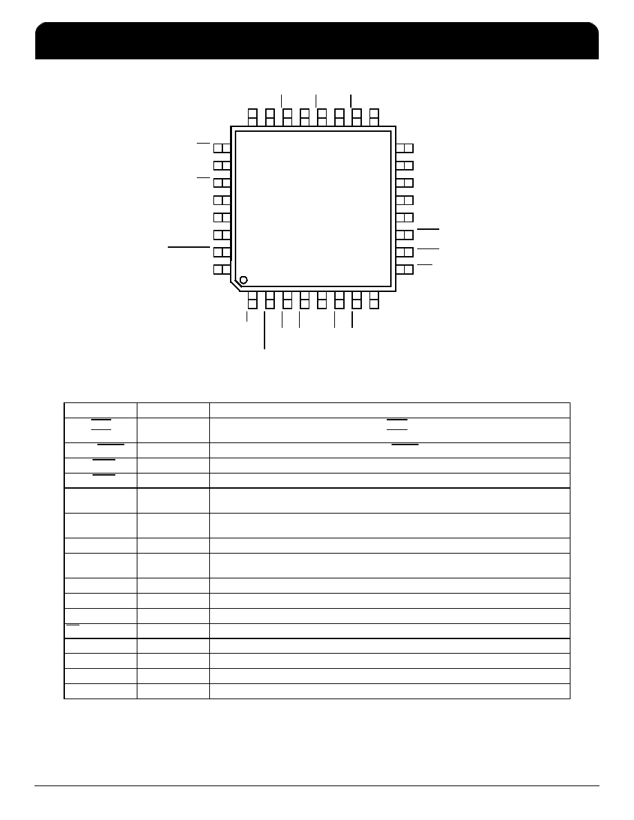
Figure 2. 32-Lead Pinout (Top View)
Table 1. Pin Descriptions
Pin Name
I/O
Pin Definition
CLK0, CLK0
CLK1, CLK1
LVPECL Input
Differential PLL clock reference (CLK0 pulldown, CLK0 pullup)
Differential PLL clock reference (CLK1 pulldown, CLK1 pullup)
Ext_FB, Ext_FB
LVPECL Input
Differential PLL feedback clock (Ext_FB pulldown, Ext_FB pullup)
Qa0:1, Qa0:1
LVPECL Output
Differential 1x output pairs
Qb0:2, Qb0:2
LVPECL Output
Differential 2x output pairs
Inp0bad
LVCMOS Output
Indicates detection of a bad input reference clock 0 with respect to the feedback signal. The output is
active HIGH and will remain HIGH until the alarm reset is asserted
Inp1bad
LVCMOS Output
Indicates detection of a bad input reference clock 1 with respect to the feedback signal. The output is
active HIGH and will remain HIGH until the alarm reset is asserted
Clk_Selected
LVCMOS Output
‘0' if clock 0 is selected, ‘1' if clock 1 is selected
Alarm_Reset
LVCMOS Input
‘0' will reset the input bad flags and align Clk_Selected with Sel_Clk. The input is “one-shotted”
(50 k
Ω pullup)
Sel_Clk
LVCMOS Input
‘0' selects CLK0, ‘1' selects CLK1 (50 k
Ω pulldown)
Manual_Override
LVCMOS Input
‘1' disables internal clock switch circuitry (50 k
Ω pulldown)
PLL_En
LVCMOS Input
‘0' bypasses selected input reference around the phase-locked loop (50 k
Ω pullup)
MR
LVCMOS Input
‘0' resets the internal dividers forcing Q outputs LOW. Asynchronous to the clock (50 k
Ω pullup)
VCCA
Power Supply
PLL power supply
VCC
Power Supply
Digital power supply
GNDA
Power Supply
PLL ground
GND
Power Supply
Digital ground
Qa1
Qa0
VCC
VCC_PLL
Man_Override
VCC
Inp0bad
Inp1bad
Clk_Selected
GND
Ext_FB
V
CC
Qb
0
Qb
0
Qb
1
Qb
1
Qb
2
Qb
2
V
CC
MR
Alarm_Rese
t
CLK0
Sel_Clk
CLK1
GND
25
26
27
28
29
30
31
32
15
14
13
12
11
10
9
12
3
4
5
6
78
24
23
22
21
20
19
18
17
16
MPC9993
PLL_EN
Ext_FB
GND
MPC9993
Intelligent Dynamic Clock Switch (IDCS) PLL Clock Driver
NETCOM
IDT Intelligent Dynamic Clock Switch (IDCS) PLL Clock Driver
Freescale Timing Solutions Organization has been acquired by Integrated Device Technology, Inc
MPC9993
2
相关PDF资料 |
PDF描述 |
|---|---|
| MSFLDL-TTL-200 | ACTIVE DELAY LINE, TRUE OUTPUT, SIP4 |
| MSFLDL-TTL-19 | ACTIVE DELAY LINE, TRUE OUTPUT, SIP4 |
| MSFLDL-TTL-21 | ACTIVE DELAY LINE, TRUE OUTPUT, SIP4 |
| MSFLDL-TTL-150 | ACTIVE DELAY LINE, TRUE OUTPUT, SIP4 |
| MSFLDL-TTL-225 | ACTIVE DELAY LINE, TRUE OUTPUT, SIP4 |
相关代理商/技术参数 |
参数描述 |
|---|---|
| MPC9993ACR2 | 功能描述:时钟驱动器及分配 RoHS:否 制造商:Micrel 乘法/除法因子:1:4 输出类型:Differential 最大输出频率:4.2 GHz 电源电压-最大: 电源电压-最小:5 V 最大工作温度:+ 85 C 封装 / 箱体:SOIC-8 封装:Reel |
| MPC9993D | 制造商:MOTOROLA 制造商全称:Motorola, Inc 功能描述:INTELLIGENT DYNAMIC CLOCK SWITCH (IDCS)PLL CLOCK DRIVER |
| MPC9993DFA | 制造商:MOTOROLA 制造商全称:Motorola, Inc 功能描述:INTELLIGENT DYNAMIC CLOCK SWITCH (IDCS)PLL CLOCK DRIVER |
| MPC9993FA | 功能描述:时钟驱动器及分配 3.3V 200MHz Clock Generator RoHS:否 制造商:Micrel 乘法/除法因子:1:4 输出类型:Differential 最大输出频率:4.2 GHz 电源电压-最大: 电源电压-最小:5 V 最大工作温度:+ 85 C 封装 / 箱体:SOIC-8 封装:Reel |
| MPC99J93 | 制造商:MOTOROLA 制造商全称:Motorola, Inc 功能描述:Intelligent Dynamic Clock Switch (IDCS) PLL Clock Driver |
发布紧急采购,3分钟左右您将得到回复。